Contents
What is a Paper Circuit?
As the name suggests, a paper circuit is a functioning electronic circuit built on a piece of paper. The item is unique because it combines aesthetics and functionality to create a paper circuit project using traditional fine art techniques.
How to Make a Paper Circuit?
Creating a paper circuit requires these four steps.
Creating Traces
Traces are the pathways or lines consisting of copper for connecting electronic components to form an electrical circuit. Paper circuit projects use tape, paint, or ink to create the traces.
Conductive Copper Tape Traces
Conductive tape is one of the most accessible options when developing a paper circuit. It also allows soldering, which is impossible with ink or paint.
Copper foil tape is the most commonly used type due to its low cost. You can get it in different sizes ranging from as thin as 5 mm to as thick as 2 inches.
On the other hand, fabric tape consists of copper, cobalt, and nickel, and its main advantage is the ability to withstand flexing/bending without breaking.
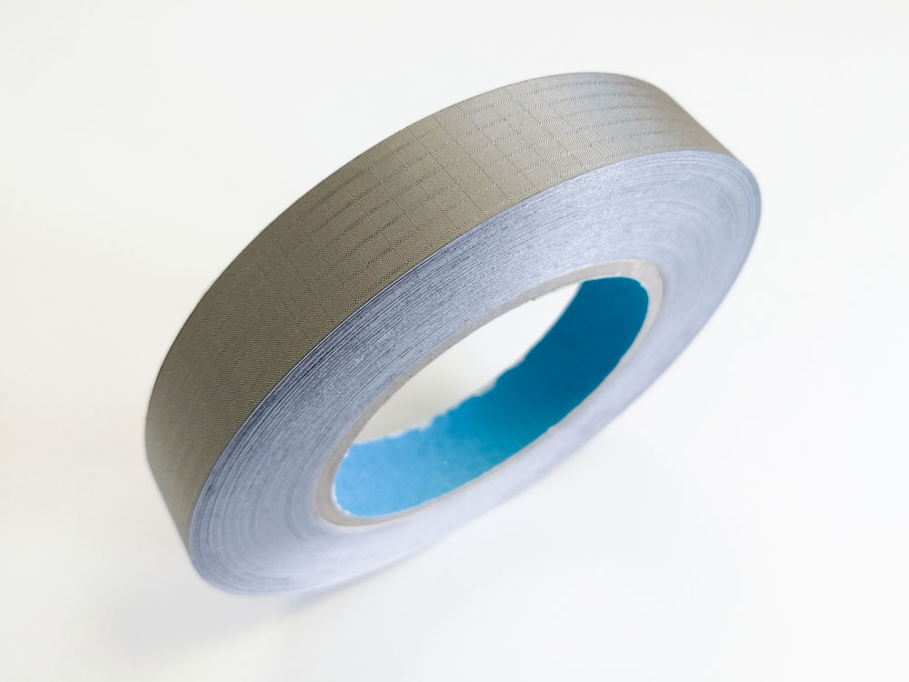
Conductive textile tape
- Peel and stick the tape by pressing it on the paper where you want it to go
- Leave spaces in the tape for the components to sit (avoid using continuous tape between circuit components)
- Use neat folding techniques around corners or cut and solder the tape
- When using copper foil tape, solder or apply clear tape on the bent leads for holding to the trace
- For fabric tape, apply conductive adhesive or sew the joint using a conductive thread material
Conductive Paint Traces
Like regular painting, conductive paints help to build artistic paper circuit projects. Most people use a squeeze bottle or brush to draw the traces while curving and swirling them to link the electrical components. Regardless of the tape, you should apply it using these steps:
Another advantage of using paint is that the conductive material can glue the electrical components to the trace. However, painting can get messy and needs a lot of drying time. Applying the paint requires the following instructions:
- Sketch the trace lines first using a marker or pencil
- Use adhesive to stick the components to the paper
- For small parts, use tweezers for accurate placement
- Apply paint along the traces and over the pads/wires
- Let the paint dry before testing
Conductive Ink Traces
Conductive ink traces usually come as pre-filled electric paint pens to simplify the drawing. Although the ink takes a shorter period to dry, fixing components is more complicated.
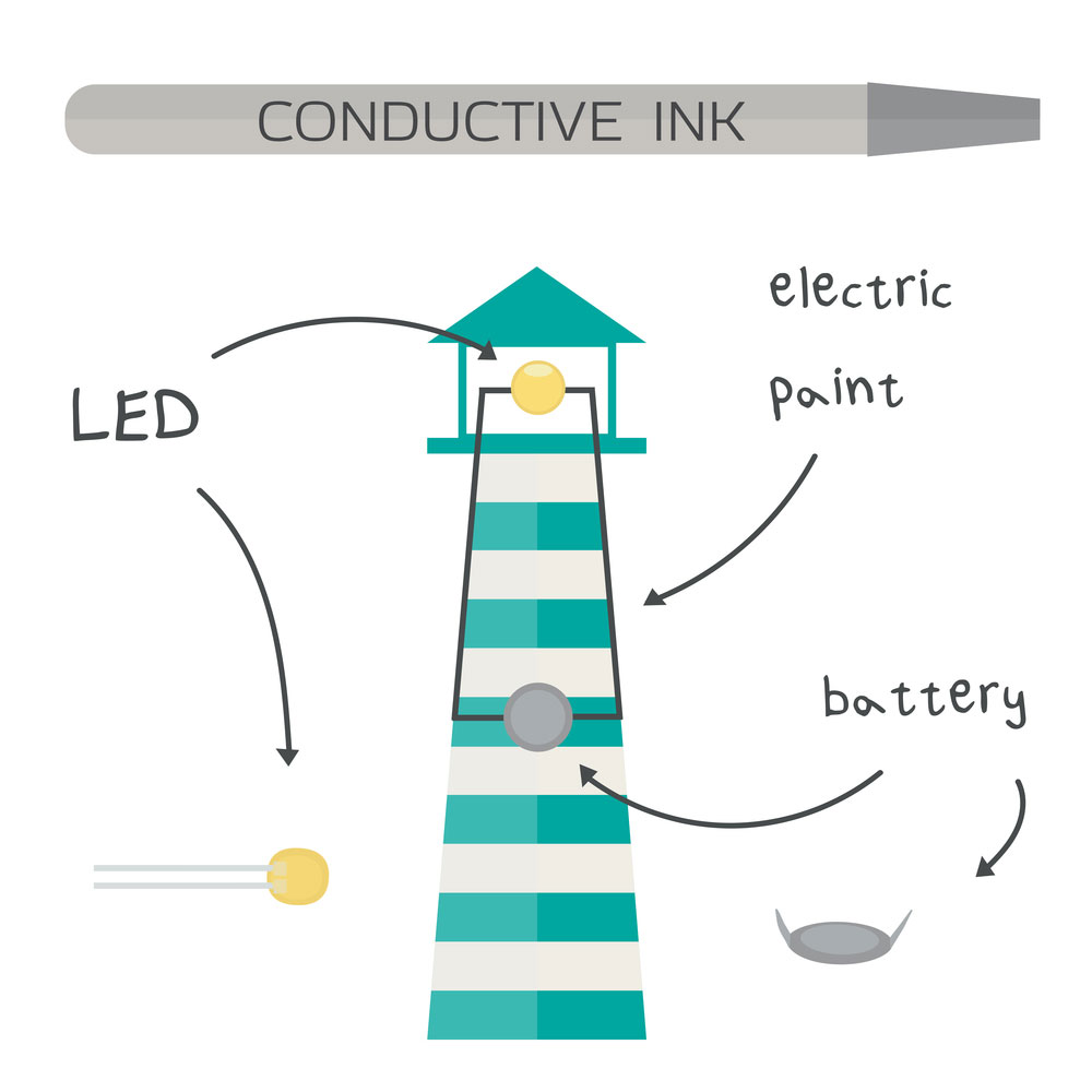
Conductive ink paper circuit
The most common pens are Circuit Scribe and AgIC Circuit Maker. For application, use these instructions:
- Use a pencil/stencil to sketch the circuit.
- If using a computer to design the circuit, leave filling outlines instead of lines because the ink does not stick well on printer toner.
- Trace the lines carefully using the electric paint pen.
- Create large pads/circles for components and continuous lines between the electronic components.
- Use conductive adhesive, circuit stickers, or tape to fix the electronic components to the ink traces.
Choosing Components
After creating the traces, the next step is to pick the components needed in your circuit, and this selection depends on the type of trace.
Through-Hole Components
Components with long leads, like LED lights, resistors, diodes, etc., fall into this category.
You can bend the leads to create more surface area to attach to the traces when using:
- Fabric tape
- Copper tape
- Electric paint
Surface Mounted Components
Working with SMD components is tricky, but their low-profile structure makes them ideal for sitting flat on a paper surface on cute cards and other paper circuit projects.
You can use these parts on:
- Conductive paint
- Copper tape
- Conductive ink
LilyPad Components
Lilypad components are perfect for paper circuits due to their low-profile design with large pads.
You can use them with:
- Fabric tape
- Copper tape
Chibitronics Circuit Stickers
These stickers feature conductive glue, making them perfect for sticking on a piece of paper.
Although they are pretty expensive, you can use conductive paint, copper tape, or fabric tape stickers.
Circuit Scribe Modules
Circuit scribe modules are magnetic and need a metal sheet behind the paper surface to connect the traces and modules temporarily.
Making Connections
After creating the traces and picking components, the next step is to connect them. There are five ways to do this. You can:
Solder
Works only on copper tape on which you can solder circuit stickers, THT, SMD, and LilyPad components.
Clear Tape
You can use clear tape to attach THT or SMD components to the copper tape.
Z-Axis Tape
Z-axis tape is a pressure-sensitive, double-sided tape that is ideal to use with components having large surface areas for connection, copper tape, and conductive ink in broad areas.
Conductive Paint
Conductive paints create cold solder joints that dry up to attach components. You can use them with THT and SMD components on non-flexible surfaces.
Conductive Adhesive/Epoxy
This option is expensive, needs an extended drying time, and some adhesives require heat setting. But it works with almost all components and traces. These include:
- Conductive ink
- Copper tape
- THT, SMD, & LilyPad components
Powering Your Project
The last step is to power your project using a coin cell battery. The tricky part is attaching the battery to the circuit and creating a battery holder. Alternatively, you can use a battery holder module or a tabbed battery.

Advances in Paper Circuit Board Research
The field of paper circuit boards has not remained stagnant. Over the years, research has led to the emergence of transparent cellulose nano paper, which functions similarly to a flex PCB substrate.
Nano paper came about after the creation of the plasma metallization process. This process converts documents into solderable circuit boards and enables the printing of memory on paper by attaching components to the cellulose substrate.
Paper Characteristics of Paper Circuit Boards
Paper is porous and can lead to problems when the conductive ink sips through and becomes segmented. There is also the issue of sintering processes, which destabilize paper.
However, all these became non-issues after a research team applied physical vapor deposition in all the fabrication steps.
Physical Vapor Deposition (PVD)
PVD converts materials from a condensed to a vapor phase and vice versa, creating a thin, condensed film at the atomic level.
The process uses either gaseous plasma or a high-temperature vacuum for the conversion. It then utilizes the pressure differences to move the vapor from the low-pressure source to the paper. The last step is to let the vapor condense on the paper to form the thin film coating.
The thin film coat is usually a solid conductive material, such as aluminum oxide, to create stable and reproducible memory devices with excellent electrical properties.
Plasma Metallization
Plasma metalization also delivers promising results because it enables the paper to function as a PCB. It uses a plasma spray head to provide a high-pressure spray containing powdered conductive metal to a silver paste-coated base material.
After the metal coats the base material, a hot plasma jet melts it to combine the two layers to create a highly conductive substrate.
Paper PCB May Lead to New Applications in the Future
Even with these advancements in paper circuits, research is still ongoing to enhance this technology and develop it for large-scale production.
Think of the possibilities. Picture having foldable, trimmable, 3D paper circuits for medical or military use. The same applies to industrial use with biodegradable PCBs.
Clearly, the field of paper PCBs shows great promise, and further research will only make it better. If you want to learn more about this technology, contact us to get insights from our team of experts.


