Let’s face it. PCB crosstalk is a massive problem the average engineer face with high-speed PCBs.
These days, we have more compact boards, making it more essential to analyze crosstalk before assembling PCBs. However, if you’re not familiar with the concept of crosstalks, it might be a bit tricky to counter.
This article will show you what crosstalk is and what you need to prevent it. We’ll also throw more light on the different types of crosstalk.
Are you ready? Let’s begin!
Contents
- 1 What is Crosstalk in PCB?
- 2 How does Crosstalk Happen on a PCB?
- 3 Types of Crosstalk
- 4 What Causes Crosstalk?
- 5 How to Reduce Crosstalk in PCB
- 5.1 1. Use only Solid Reference Planes.
- 5.2 2. Use Back-drilled Vias
- 5.3 3. Check and Limit Crosstalk
- 5.4 4. Go for Differential Pair Routing
- 5.5 5. Separate High-Frequency Signals
- 5.6 6. Correctly Eliminate Odd and Even Mode of Transmission
- 5.7 7. Utilize Short Traces
- 5.8 8. Separate Asynchronous Signals
- 5.9 9. Reduce Parallel Trace Runs
- 5.10 10. Utilize Guard Traces
- 5.11 11. Use Orthogonal Routing
- 5.12 12. Keep your Traces Separated
- 6 Final Words
What is Crosstalk in PCB?
PCB crosstalk is an unwanted energy coupling between traces. It causes a trace’s signal pulses to override another trace even if they’re not in physical contact. It usually happens when you don’t correctly space your parallel traces.

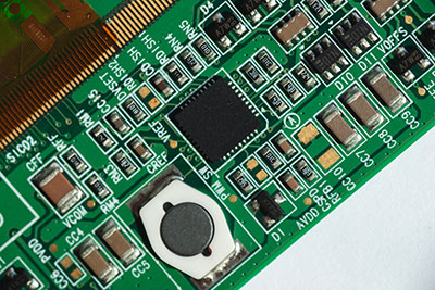
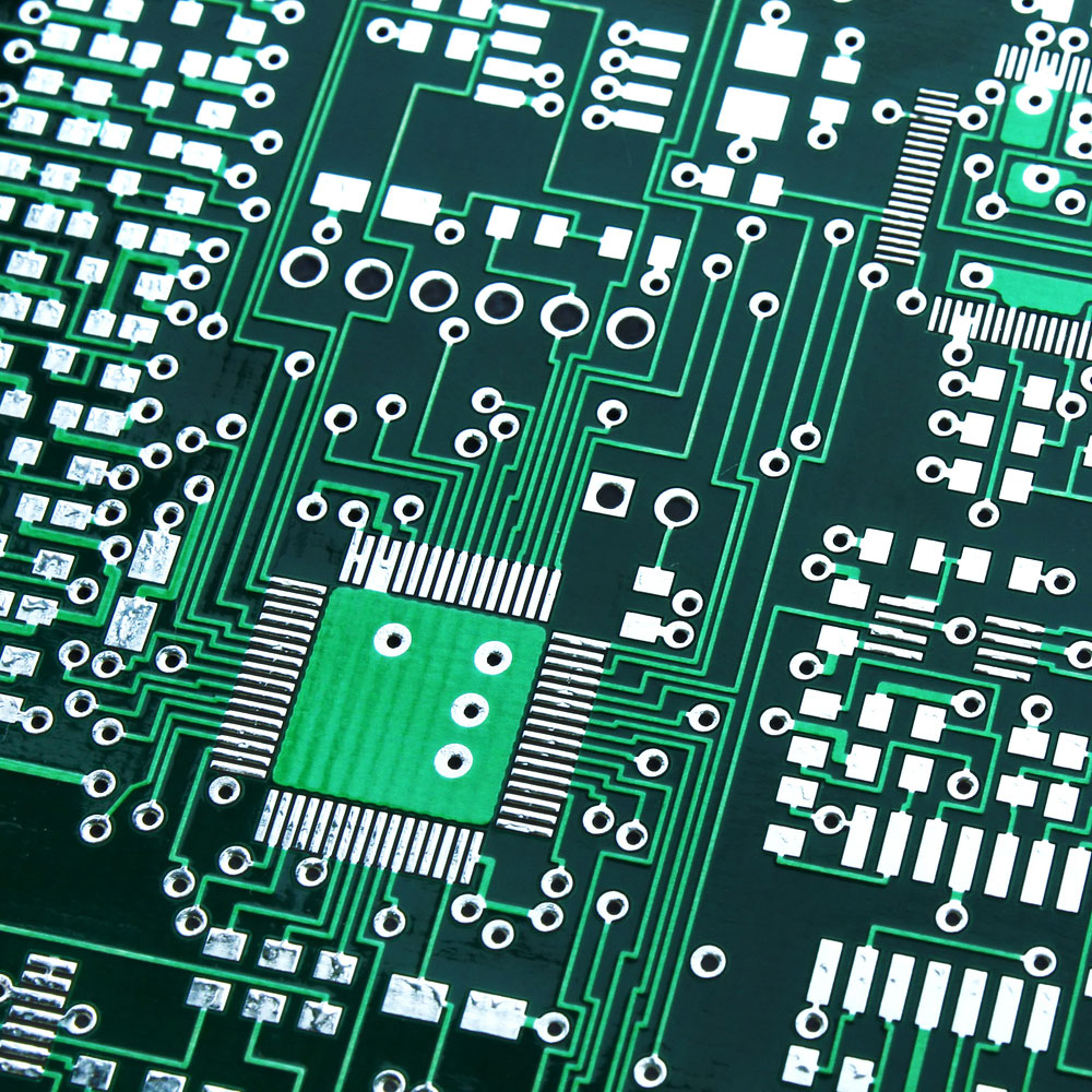
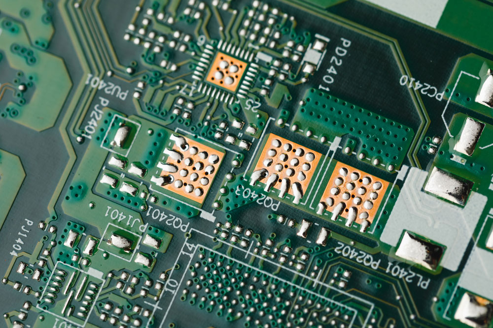
PCB Traces
Though you might argue that your designs keep to minimum spacing requirements, it may not be enough to prevent electromagnetic coupling.
So, think about two parallel traces on a PCB; If one trace has a higher amplitude, it could affect the trace with a lower amplitude. As a result, the weaker trace’s signal starts copying, the stronger signal instead of transmitting it. That’s when crosstalk occurs.
In truth, mutual inductance causes the transfer of current from the strong to the weak trace. Then, the capacitor created from the mutual capacitance makes the current similar, which can affect a circuit’s signal integrity.
Many designers believe that crosstalk results from parallel lines on the same layer. But, it can also occur in adjacent lines on different layers.
Moreover, controlling or preventing crosstalk can be tricky, mainly when it stays undetected. And if you don’t deal with it at the initial stage of your designs, it would downgrade your PCB’s functionality.
How does Crosstalk Happen on a PCB?
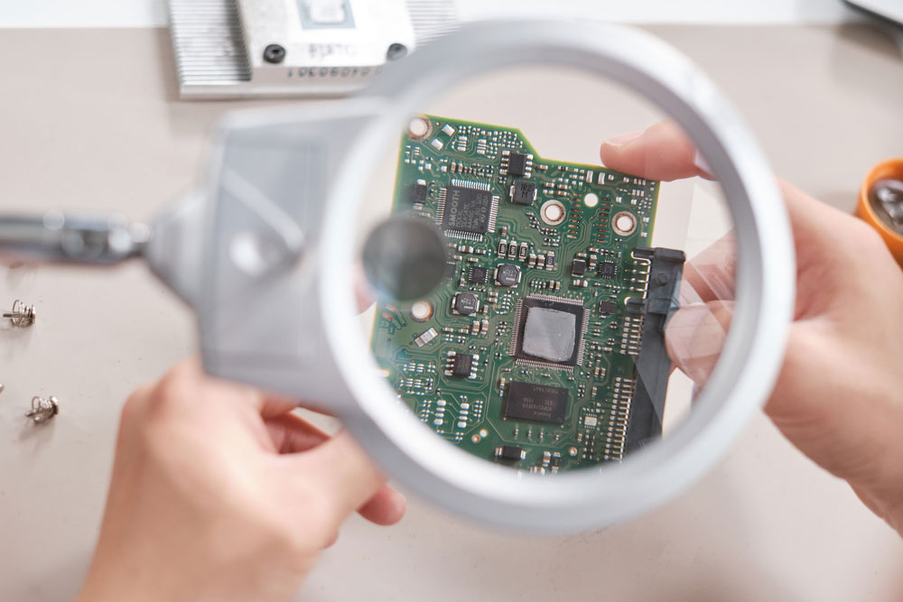
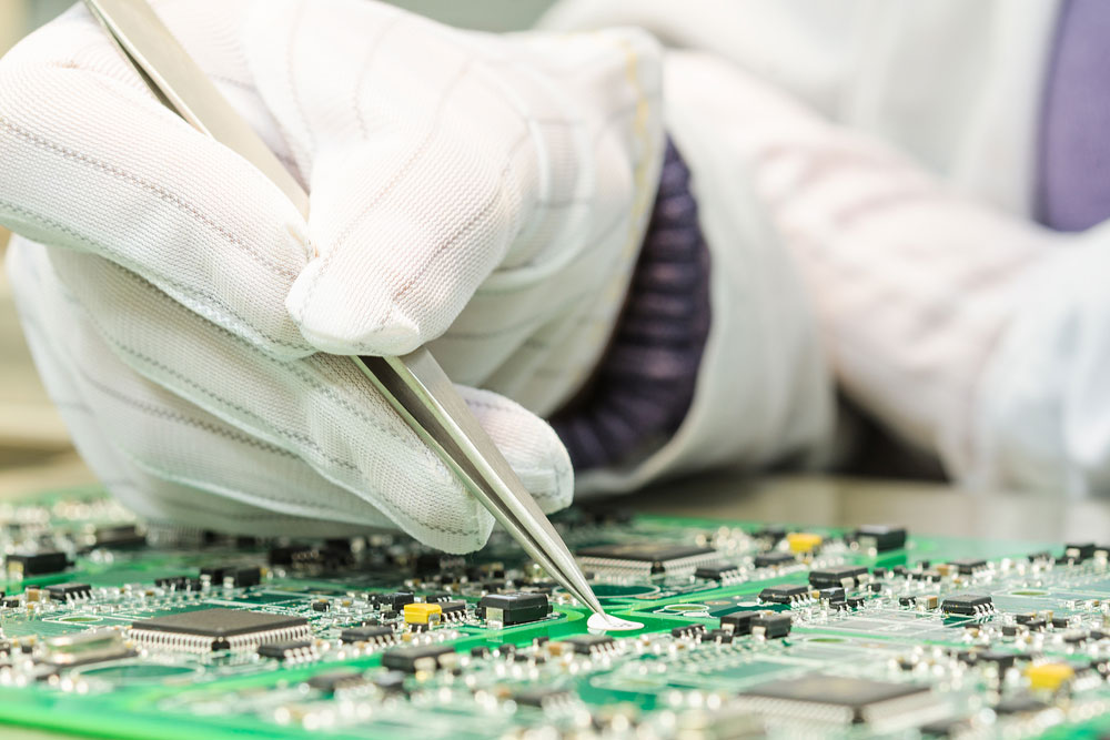
Hand Inspecting PCB
There are usually two ways crosstalk can happen in a circuit: Common impedance coupling or electromagnetic coupling. Common impedance coupling is easy to analyze and only occurs when various signals share one return path.
On the other hand, electromagnetic field coupling is more complex and has two sub-divisions: inductive and capacitive.
Capacitive Coupling
Parallel traces are the capacitor parallel plates of a high-speed PCB separated by a dielectric. And the electric field between the strong and weak trace is what we label the capacitor.
Now, if there’s a change in capacitor voltage, it’ll alter the electric field and generate a displacement current. This displacement current causes a capacitively coupled current, leading to crosstalk. We call this effect parasitic capacitance.
Inductive Coupling
Inductive coupling depends on the number of magnetic field rings revolving around the weak trace. The stronger trace’s magnetic field surrounds the more vulnerable line and changes its transmission current.
When this happens, the stronger line induces voltage according to Faraday’s law of induction. The induced voltage is what transmits the current in the form of crosstalk.
Broadside Coupling
Broadside coupling happens when parallel traces run close to adjacent layers. Plus, it’s more likely to occur when a small amount of core thickness separates these adjacent signal layers. Usually, it’s 0.1 millimeters (4 mils), which is not nearly enough for spacing two traces on the same or adjacent layer.
Types of Crosstalk
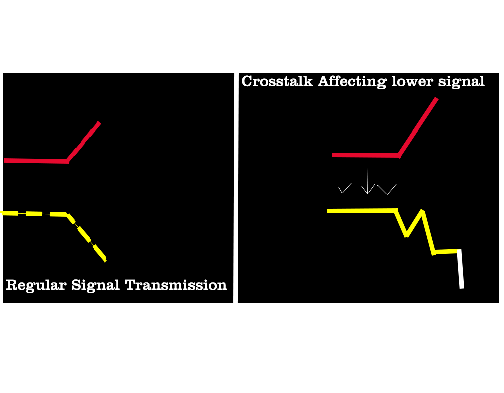
Crosstalk Affecting Signal Transmission
We can classify various crosstalk types into propagation direction, measurement zones, and quantification. Let’s take a closer look.
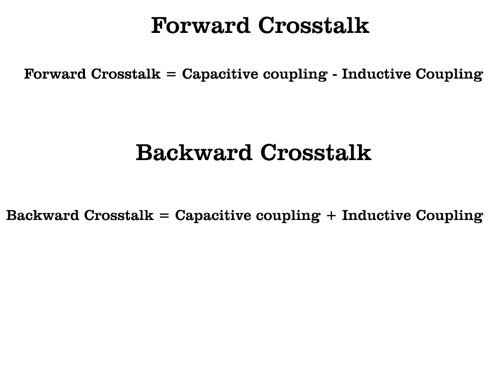
Based on Propagation Direction
Under this classification, we have two crosstalk types, including forwarding and backward crosstalk.
For forward crosstalk, the more vulnerable trace transmits the copied current in the stronger signal’s direction. Contrarily, backward crosstalk means the copies signal transmit in the opposite direction.
Here are the formulas for crosstalk based on propagation direction:
Based on Measurement Zone
There are also two crosstalk types under this classification. They include:
- Far-end crosstalk (FEXT): refers to the interference on the weaker trace’s receiver side.
- Near-end crosstalk (NEXT): refers to the noise n the weaker trace’s driver side.
Also, these crosstalk types can happen anywhere on a trace. So it doesn’t matter if it’s a single-ended or dual conductor.
Based on Quantification
Here, we have three crosstalk types, which include:
- First, Power-sum-FEXT (PS-FEXT): refers to the absolute influence of far-end crosstalk.
- Second, Power-sum-NEXT (PS-NEXT): refers to the relative effect of near-end crosstalk.
- Third, Power-sum-equal-level-crosstalk (PS-ELFEXT): refers to the addition of PS-NEXT and PS-FEXT.
Alien Crosstalk
This crosstalk is more complicated than other variants. It’s hard to eliminate, and shielding won’t provide enough protection. It happens when different signals corrupt the weak signal.

What Causes Crosstalk?
Measuring Crosstalk
Here are some factors that can cause PCB crosstalk:
- Cross can be a result of propagation velocity differences. However, you can mitigate it through propagation delay and trace length matching.
- Increased data rates can also cause crosstalk. A board that has high data rates will also have high rise times. And Faraday’s law states that a higher rise time will increase crosstalk.
- Stubbed PCB vias is another factor that can generate crosstalk. They create reflections and ringing, causing crosstalk.
- Board size: a larger board will require longer traces. But longer traces can cause crosstalk—because they act like antennas.
How to Reduce Crosstalk in PCB

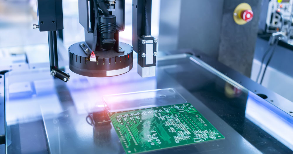
High-speed PCB
You can’t always avoid crosstalk in high-speed PCBs. But you can reduce it to an insignificant level. Here are some methods you can use for this task.
1. Use only Solid Reference Planes.
Solid reference planes can absorb the overflowing magnetic and electric fields. Hence, it won’t spread and corrupt other signals.
2. Use Back-drilled Vias
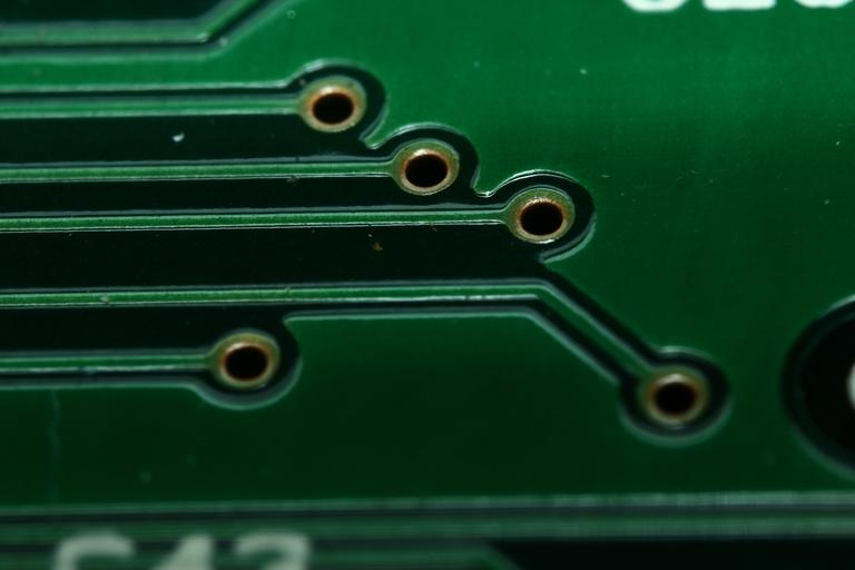
PCB with Vias
Avoid using via subs as they can dampen signal integrity and cause crosstalk. Instead, go for back-drilled vias.
3. Check and Limit Crosstalk
Measure your board’s crosstalk and ensure it doesn’t go beyond 150mV. Also, avoid adjusting your signal rise time. It could increase crosstalk and potentially set it past the limit.
4. Go for Differential Pair Routing
Using tightly coupled differential routing can help reduce crosstalk. How? Since there is no equal coupling, the differential pairs won’t accept the common mode noise, which mitigates crosstalk.
5. Separate High-Frequency Signals
Man working on PCB
Avoid placing high-frequency signals near other signals. Separating them would help reduce the chances of crosstalk.
6. Correctly Eliminate Odd and Even Mode of Transmission
You can use a three resistor network or T-termination to cancel the even and odd transmission mode effectively.
7. Utilize Short Traces
PCB with Traces
Source: Snappy Goat
Put, the longer your traces are, the higher the chances for crosstalk. However, keeping traces short can help reduce coupling and mitigate crosstalk.
8. Separate Asynchronous Signals
Always keep asynchronous signals far away from high-frequency signals. Try placing them closer to power lines to reduce the possibility of crosstalk.
9. Reduce Parallel Trace Runs
More prolonged traces (over 500mils) will increase mutual inductance and cause crosstalk.
10. Utilize Guard Traces
You can use guard traces to mitigate crosstalks between transmission lines. However, these traces are tricky and make routing complicated.
11. Use Orthogonal Routing
If you’re working with adjacent signal layers, try routing them orthogonally. It would help to reduce capacitive coupling between the layers.
12. Keep your Traces Separated

Well-spaced Traces
Source: Snappy Goat
Use the 3W rule to space all your traces correctly. If you don’t stick to this rule, you’ll get an increased mutual capacitance, which leads to crosstalk. But using the 3W law will help minimize crosstalk by 70%.
Note: You can get a 98% crosstalk reduction by using the 10w rule.
Final Words
PCB
Crosstalk is one of the inevitable problems of high-speed PCBs. Unfortunately, it’s impossible to eliminate from your board, but you can reduce it to a level that keeps your signal integrity and circuit performance safe.
Crosstalk is the result of unintentional coupling between parallel or adjacent traces. But you can minimize the chances of coupling by correctly spacing your lines.
Remember that there are various ways to reduce crosstalk, so be sure to use one that fits your circuit design.
Feel free to contact us if you have any questions.


