Contents
- 1 PCB Fabrication Process
- 2 PCB Fabrication Product Design
- 3 PCB Fabrication Process Product Material
- 4 PCB Fabrication Final Environment
- 5 PCB Fabrication Test Compliance
- 6 Common Errors in PCB Fabrication
- 7 PCB DFM can also help save costs
- 8 PCB Fabrication Advantages of DFM
- 9 Develop DFM Rules With Your PCB Supplier
- 10 Summary
PCB Fabrication Process
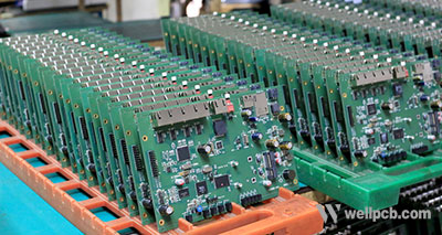
PCB Fabrication Process the first part of DFM aims at determining the correct types of manufacturing steps to use for the product in question. When you want to produce PCB boards at specific quantities, the process must reflect the production scope and the number of pressings that you plan for the run.
DFM helps you determine some of the best PCB manufacturing processes, such as the size of the materials used, the steps required on the PCB surface, and other auxiliary steps. As it appears, DFM saves a lot of time during the production process and saves on PCB fabrication costs.
PCB Fabrication Product Design
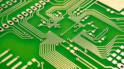
When it comes to PCBs, the second part of DFM is examining the design of the product and determining whether the specs will eventually suit the final finished product. It also determines whether changes are necessary before commencing with a full production run. This step’s primary purpose is to amend any possible issues to do with design so that production runs smoothly and efficiently.
If you choose to revise a design currently existing, it is essential to ensure that you adhere to fundamental design principles. As a buyer or distributor, you need the entire decisions at this stage with your potential manufacturer. Doing this, especially during PCB fabrication and assembly, will see you producing PCBs according to your product’s manufacturing principles.

PCB Fabrication Process Product Material
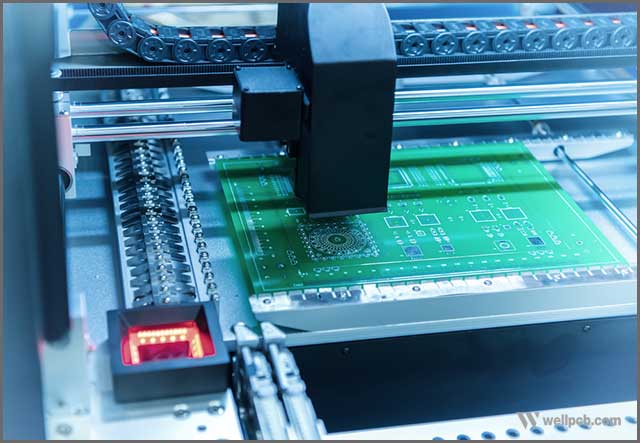
Another advantage of ensuring that you stick to DFM during PCB fabrication assembly is that it helps PCB designers determine the necessary materials for the product in question. Depending on the shape of the product, the size, and the intended use, you’ll need to factor in several aspects such as texture, strength, thermal properties, and other elements required for your products.
As a buyer or distributor, you will have to make consultations with your contract manufacturer. It is a process aimed at making sure that the chosen materials used in the manufacture of your printed circuit boards meet the final production run’s requirements.
But if you have a particular material in mind, then you will have to be aware as to whether that type of content will be able to withstand heat while being able to conduct electricity effectively. The reason for this is because such factors could make or break the product.
PCB Fabrication Final Environment
Before finalizing your choices towards the method, material, and design of the final product, you will first have to study or factor in the situations in which your consumers will be using them. The moment you finish determining the impacts that the situation might have on the product’s shape and material, you will then have to examine whether DFM choices will come up.
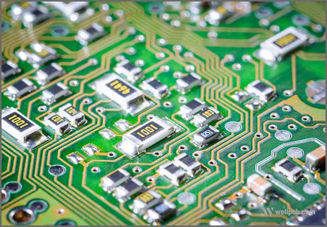
Here, an apt example of design for manufacturing includes considering where and how your consumers will be using the printed circuit board. For example, if you choose to develop products that will find use in outdoor environments throughout the year, then the materials that you select should be in a position to withstand severe environmental conditions.
It means that the design should be able to accommodate several setups. With the design for manufacturability, you will be better positioned to manufacture products that will function as initially stated in the environment where they are supposed to work. It is another significant advantage associated with implementing design for manufacturability mechanisms in producing printed circuit boards, regardless of whether you are thinking of multilayer PCB fabrication or low-cost PCB fabrication.
PCB Fabrication Test Compliance
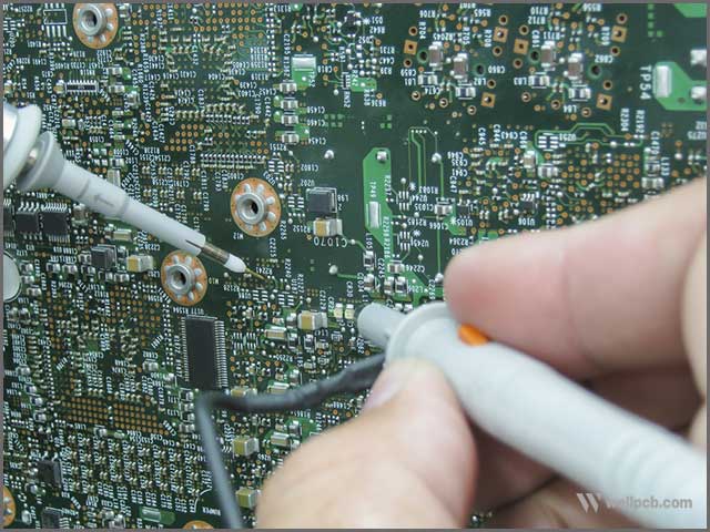
Another significant benefit associated with design for manufacturability, especially when it comes to the manufacture of printed circuit boards, is that it helps determine whether the materials and design of the product will satisfy the quality and safety standards of several entities with interest in the product.
For instance, a third-party ISO-certified facility for testing can help in determining such. Again a neutral manufacturing expert should be the one to oversee the trial. Several entities may have their standards that would impact your capability of surging ahead with a particular design that you may currently have.
Perfect examples are regulatory rules at the state, federal, or international level that may deem your products unsafe in its current state. Such regulations may claim that your product doesn’t meet the code of the intended industry or specific safety standards required. However, by implementing design for manufacturability, you’ll be avoiding such risks, thereby saving a lot of time and money.
Common Errors in PCB Fabrication
DFM is another vital tool that can help you to eliminate mistakes during PCB design and production. DFM can assist you in the following ways:
• Edge clearance – failure to allow edge clearance Is a big mistake that PCB designers make. It can be problematic for copper found along the edges of a PCB since copper may corrode without a protective coating.
• Acid traps – these are recurring issues that PCB designers fail to consider. It is advisable to avoid designing angled traces at acute angles.
• Complex layout – if you arrive at a situation where your board is involved, you may have to rethink the design, costing you more.
• Lack of solder mask – solder mask are essential elements that prevent any contact between copper and other materials. Lack of it may cause short circuits.
• Component spacing – with tight spacing, you may be tempted to add vias as means of freeing up some space. Unfortunately, this may end up weakening the mounting capabilities of your PCBs.
In short, implementing DFM will see you avoiding all the above errors that may end up being costly and time-consuming on your end.
PCB DFM can also help save costs
Manufacturing printed circuit boards are not as cheap as you can imagine. The manufacture of printed circuit boards from the board layout, design all the way to having a final product is a complicated and expensive process. Once again, no one wants to operate in an environment where losses are second only to damages, and profits can only achieve once a day.
Just like any other business entity, printed circuit board manufacturing firms are in business to make money and minimize costs. There are plenty of tricks and different strategies for realizing profits and reducing costs, with the design for manufacturability being one of them.
By implementing design for manufacturability, printed circuit board companies will realize lower manufacturing costs. Here, they’ll have the assurance of reliable board design, some significantly reduced turnaround time, faster bring up of results, improved quality, and lower overall costs towards product development.

PCB Fabrication Advantages of DFM
The design for manufacturability and assembly is an essential part of any product development cycle. Wne all are all aware that saving even the slightest time off in the development cycle of a product can help you get to the market faster. Better yet, design for manufacturability ensures that your products can undergo manufacturing at the agreed time and date.
That’s not all regarding DFM. Design for manufacturability ensures that you eventually roll out products that will meet the demands of the market. Sometimes, DFM involves the optimization of the model of products, both for its manufacturing and assembly.
By going ahead to employ design for manufacturability tactics, printed circuit board designers are more than likely to witness a reduction in the production of their printed circuit boards while maintaining quality at the same time. The benefits of design for manufacturability do range from the apparent quality, delivery, and cost-saving to several important and refined benefits such as:
1 Lower manufacturing costs
2 High-quality goods
3 Faster time to market
4 Low capital equipment cost
5 Few engineering changes
6 Factory availability
7 Greater automation
8 Faster production speeds
9 Helps in checking for a pin to pad or pad to pad geometry
10 Assists designers to check for incorrect spacing
11 Contributes towards the identification of overlapping components
Develop DFM Rules With Your PCB Supplier
If you are unsure whether the design of your PCB will come out as you intend, you may have to develop a couple of DFM rules with your supplier. By developing DFM rules, you have the assurance of high-quality boards that will undergo manufacturing as agreed. There’s no reason for believing in your supplier’s
DFM rules only to be presented with products that fail to satisfy you in the end. Another advantage of DFM is that it gives you room to strike an agreement between you and your supplier. This way, you are assured top-notch products that will function as you want them to do. Additionally, by having rules in place, you are assured of compensation if your supplier ends up disappointing you.
Summary
When it comes to compliance testing and design inspections, you need to seek the input of a qualified and objective third party. At WellPCB, we run complete design for manufacturability analysis on all printed circuit board designs and prototypes that we may have to detect and identify problems.
Feel free to circuit board shopping, various things might get you confused. Whether you are going for a single-sided PCB, a double-sided PCB, or any other type of PCB, You can contact us today and learn how to assist you in improving your printed circuit boards before putting them into full production.
