When you think of transmission lines, cables come to mind. Though that’s not what we’re focusing on, a PCB transmission line acts similarly. While regular cables transfer electricity from one point to the other, PCB variants transmit signals to & from the receiver and transmitter.
But, adding transmission lines to your PCB layout may be tricky if you’re unfamiliar with the process. Luckily, we’re here to provide all the necessary details before you attempt to integrate them into your subsequent high-speed designs.
This article will discuss PCB transmission lines, the different types, their importance, and more.
Contents
What are PCB Transmission Lines
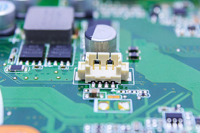
Printed circuit board
PCB transmission lines are interconnections you can use to transfer signals from your circuit board’s transmitter and receiver. Usually, they host two conductors, including a signal trace and return path. Also, dielectric material makes up the thickness (like PP, Coverlay, & Fiberglass) between these conductors.
Further, all I/O signals move through PCB transmission lines. Single-ended I/O interfaces utilize the signal trace and reference plane to transfer a signal from one point to another. But differential I/O creates transmission lines by combining two traces with a reference plane.
What are the Types of Transmission Lines?
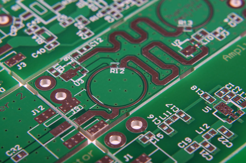
Typically, PCBs have two primary signal transmission lines: striplines and microstrips. Microstrip transmission lines have one uniform trace on the board’s outer layer. Further, this single trace also runs parallel to the PCB’s ground plane.
What’s more? The ground plane supplies a return path for the traveling signal. Also, a certain height of dielectric material helps keep the trace and ground plane separated to avoid contact.
On the other hand, stripline transmission lines have one uniform trace inside the circuit board’s inner layer. Also, parallel dielectric layers and conducting planes separate the trace on each side, providing the transmitted signal with double return paths (reference planes one and two).
Beyond these conventional types, you can use a third type on your PCB (though it’s incredibly uncommon). We’re talking about coplanar transmission lines. This waveguide structure hosts the return path and signals trace on the same board layer.
However, the signal trace stays at the center, with two adjacent outer ground planes surrounding the trace. Also, you can find the dielectric material underneath the transmission line structure. In addition, microstrips and striplines can use coplanar structures.

Why are Transmission Lines Important in PCBs?
Transmission lines are essential to prevent serial link losses and subsequent expenses. Such measures are particularly true for high-frequency PCBs with higher chances of dielectric losses and signal disruptions.
As a result, you must carefully study and finalize your transmission line’s format & modeling in the design phase. Thankfully, advanced technologies in fabrication increased operating frequencies, and integrated circuit modeling allows you to implement digital circuit designs in RF and microwave connections.
Tips to consider when Designing Transmission Lines
Before connecting traces on your PCB design, it’s necessary to consider a few parameters. Here are a few tips to help in this regard.
- Transmission lines are networks of two or more ports hosting power generation and receiving ends. As a result, most transmission lines must have at least conductors.
- If you have three-phase lines, then you’ll need three conductors. Also, you can use typical PCB traces or coaxial cables as transmission lines.
- Transmission lines will behave differently in short wavelengths and small circuit sizes. In addition, the capacitance between the two conductors at a specified length and loop inductance over the conductor’s length will also influence behavior.
- While you may think transmission lines move signals through different points, that’s not all you must consider. Although that’s the essential function, we recommend designing your transmission line carefully. Otherwise, loopholes in your trace and transmission line designs will affect the PCB’s functionality.
Rounding Up
Impedance is one of the crucial factors to consider when designing PCB transmission lines. Otherwise, signal reflections will interrupt the entire process if the impedance fails to match the line’s length.
So, it would be best if you calculated your PCB design’s physical characteristics to control your trace line’s impedance, allowing the system to maintain a consistent value.
Do you have more questions on this topic? Be sure to reach us, and we’ll be happy to help.


