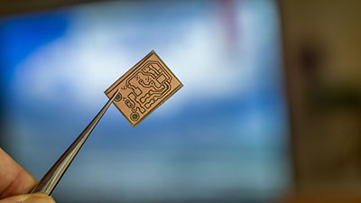
PCB Via comprises copper cylinders that connect pads, traces, and polygons on two PCB layers together through thermal or electrical connectivity. Via allows the passage and distribution of thermal and electrical energy between PCB layers.
For instance, the more the amount of energy a PCB layer can transmit, the more Via it should have. The design and development process for PCBs Via is, therefore, critical.
Every PCB designer should understand the types of PCBs Via that exist, their effects on the board, and when they could be useful. These, and many more, are what this article would teach us. Let us take a look at these tips that, if used, will give you the best PCB design.
Contents
- 1 Options Of Via
- 2 What Kind Should I Use?
- 3 The Size Should Via Be?
- 4 Conductive Fill or Non-conductive Epoxy Fill?
- 5 Make Minimal Use Of Stacked Via For Internal Layer Routing
- 6 When To Use Blind and Buried Via in My Design
- 7 Tips When Using Tented Via
- 8 Tips When Using Via-in-Pad
- 9 Make Use of a Manufacturer That Can Successfully Achieve Your PCB Design
- 10 Conclusion
Options Of Via
There are three main types of Via: Blind Via, Buried Via, and Through Via.
1. Blind Via: is found between exterior and interior PCB layers, connecting one to the other.
2. Buried Via: is found between two interior PCB layers, connecting one to the other.
3. Through Via: is found between two exterior PCB layers, connect one to the other.
Other types of PCBs Via include:
1. Micro Via: a complicated PCBs Via option used for variable-length connectivity for high-density interconnections.
2. Via-in-pad: is the most complex PCBs Via option between two external board surfaces or between an external board and internal board connectivity, used to route components with exceptional pitch angles.

What Kind Should I Use?
Through Via are adequate for two-layered PCBs; for more complex PCBs, you can consider using embedded Via and blind Via. Via is the most cost-effective and reliable of the three, while Buried Via is the most expensive and the least secure. In addition to their reliability problems and costly nature, Buried Via is challenging to troubleshoot.
Due to its low cost and high reliability, some manufacturers often use Through Via instead of Blind Via PCBs. But this method leads to the creation of unneeded holes that can interfere with other connections in-between the PCB layers. Blind Via, on the other hand, will only create unnecessary holes in-between the two layers being connected.
In the end, consider all options available for your PCB design purpose and opt for the best choice.

The Size Should Via Be?
Although you can specify any Via size, let the Via on your PCB be the same size. If you use different Via sizes, then you will have to use different drill sizes. Each manufacturer has its minimum drill diameters, and they may not accept your job if you choose a width that doesn’t fall into their capabilities.
If you’re specified Via size is too big, it will consume a lot of PCB real estate and makes routing difficulty and the PCB manufacturing more expensive. If you’re specified, Via size is smaller than your manufacturer’s preferred minimum diameter size. You will make the job more difficult for your manufacturer, making the whole process more expensive for yourself. Your best bet is to get a Via size greater than or equal to the preferred minimum Via diameter of many manufacturers so that you don’t get stuck with one manufacturer.
If you have a preferred PCB manufacturer, ask them about their preferable minimum drill size or check the company’s website’s capabilities section to be sure of your Via choice.
The best place for many small Via PCBs boards, but not all large PCBs Via is placed after all the heat conduction and heat conduction. The problem is, the whole board will fail the moment the single massive Via fails.

Conductive Fill or Non-conductive Epoxy Fill?
Non-conductive fill is more cost-effective and is sufficient for most PCB signal routing projects than conductive fill. Non-conductive epoxy fill is preferable in most instances than conductive fill. Unlike conductive fill, non-conductive fill prevents board fracture and failure, contracting and expanding accordingly as the PCB cools and heats, respectively.
Conductive fill is preferable as a PCB thermal Via when thermal conductivity is of utmost importance, as non-conductive epoxy interferes with thermal conductivity between the boards. Unlike the name suggests, a non-conductive epoxy fill can transmit electrical energy through its copper-plated surface without interference.

Make Minimal Use Of Stacked Via For Internal Layer Routing
Stacked Via is a PCBs Via option used in place of Blind Via due to a routing problem that makes sequential lamination impossible. Subsequent lamination problems may arise if a Blind Via’s termination layer is situated where another Blind or Buried Via is located.
The advantage of Stacked Via is that it provides more space for PCB routing, as several Via can be stacked on each other. However, stacking different Via on the same spot can weaken that particular part of the board and lead to board failure.
Endeavor to make minimal use of Stacked Via for internal routing because their fabrication requires much more precision than other Via options.


When To Use Blind and Buried Via in My Design
Wire routing called a path follows the active component “placement step” in assembling PCBs or Integrated Circuits (ICs). It involves the connection of all the active ingredients on the board using wires.
A high-speed PCB design is usually affected by the board’s physical features, such as connection, component layout, and housing. These physical features generally influence the integrity of a high-speed PCB.
Use Blind or Buried Via in your PCB design when routing PCBs with high-speed signals such as High Definition Multimedia Interface (HDMI). This way, the integrity of the signs and component connection is much more protected.

Tips When Using Tented Via
Some Via does not extend to the PCB surface (for example, embedded Via). While some extend to the PCB surface (for example, Via). PCBs Via that extends to the board surface is either closed or opened. Closed PCBs Via is called tented Via.
When PCB manufacturers use solder to cover the Via holes to reduce the number of exposed pads on the board, a tent Via made.
Ensure that your tented Via is as flat as possible to prevent tombstoning or solder bridge. A situation in which some of the active components separate when soldered.

Tips When Using Via-in-Pad
Via-in-pad is difficult Via option to route, taking more time, and demanding more money. However, it also has its advantages. Via-in-pad routing is adequate when you have a board size limitation. routing option restriction, or limitation of connection points on your PCB components. Therefore, this type of path is useful for Ball Grid Array (BGA) and Chip Scale Package (CSP).
When it comes to a Via option, your best bet is to choose the least complicated option that can serve your needs. In line with this, make Via-in-pad your last resort as it is the most complex of them all. Only use it when other PCB routing options cannot suffice for your PCB needs. When making your PCB decisions, consider your PCB needs, the board’s reliability, signal integrity, and board manufacturability.

Make Use of a Manufacturer That Can Successfully Achieve Your PCB Design
As you can see, there are many points to consider for a Via PCBs option. From your size requirements to your PCB needs and complexity. Your choice of a PCB manufacturer will determine your project’s success.
Research the capabilities of potential PCB manufacturers available to you. Compare the financial cost from each of the manufacturers. In the end, ensure you choose a manufacturer that can successfully make your PCB design on budget and on time.

Conclusion
Selecting the best PCBs Via option may seem like a daunting task to many PCB designers. but every designer can find relief by following the nine tips outlined above.
There is no reason to worry about making the right PCB decisions if you buy your PCBs from WellPCB. At WellPCB, we know all the rules and tips on making the best PCBs Via that can serve your needs. Feel free to contact WellPCB.