Contents
PCB vias can Affect Signal Integrity
Under normal conditions, you want to route the message so that the return current passes through the ground plane, which is located directly beneath the line, ideally. It is also what happens in a balanced impedance-controlled transmission line. However, if a PCB Vias comes in the way, the return current must find the transition path itself. It will need to cross layers and go to the area with the closest grounded PCB vias.
So, if the return current covers any extra distance, it delays the high-frequency signal. It is because of the creation of an inductive loop due to additional PCB vias. It is not just that; and you may also accumulate unwanted signals along this route.
Furthermore, PCB vias also degrade signal integrity because of long delays and the significant rise and fall periods. You can study S parameters to assess the effect of vias on signal integrity. They reflect the properties of all channel components, including failure, attenuation, and reflection, etc.
To improve signal integrity, keep your PCB via count to a low number in case of high-frequency signals. You will get a quick rise time and a shorter time delay. If you add smaller PCB vias, they can give your shorter delay but do not significantly affect the rise time. Lastly, you can also ensure to decrease the length of the PCB vias. It will also lead to a quick rise time and less time delay.
PCB vias to Prevent High-frequency Signal
PCB vias function similarly to those emergency drains: water must flow through a cylindrical pathway around the plug from a flat surface. The water cannot teleport to the sewer because the drain is resistant to the sea. PCB vias drive the current to a ring-shaped pathway from a flat copper track.
The sink connection here is the core of the non-conductive gas, air. Henceforth, you are forcing the current to flow through the metallic ring about the hole. The PCB Via refuses the current flow and behaves like a parasite inductance, which affects the high-frequency signal performance.
The plating thickness on PCB vias is also shallow, which provides a great deal of resistance. So, this property also does not let it to carry much current. You would need several of them to handle the high flow.
This current may be flowing from one side of a board to the other. It would waste space as well.
On the bright side, you can also find PCB via calculators online. If you add the size of PCB vias that you plan to use, online calculators will see their total resistance. You can also get to know their current carrying capacity and some other parameters.
High-frequency PCB Vias Require Special Testing and Design
If you keep adding PCB Vias into your PCB design, you are also creating problems for the PCB manufacturer. The process control that the PCB manufacturers use to manufacture basic PCBs is not appropriate for the PCB vias plating process’s quality control.
In other words, you cannot precisely predict the PCB vias for high-frequency signals. It is not possible without strict controls in the development stage. It requires additional design time and testing for efficient working of high-frequency PCBs in the final assembly.
PCB manufacturers also use automated drilling machines, which increases the manufacturing cost of your PCB vias. Although you cannot directly see it on the bill, so we would recommend that you keep the copper trace on the same layer in case of high-frequency signals.
PCB Vias Lead to Impedance Mismatching
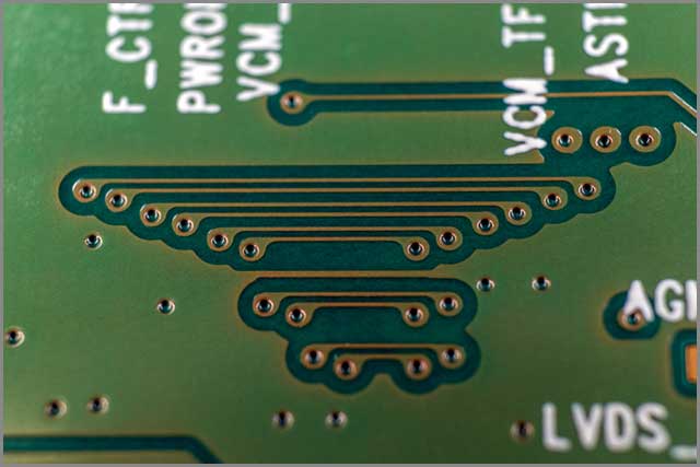
More PCB Via for high-frequency signals will also cause impedance mismatching. This impedance discontinuity further results in reflections. You can imagine a cable such as a fiber-optic that substitutes light with electrons. When everything is nice and smooth, light enters one side and exits the other in a fiber-optic cable.
However, if you have a break in the wire or portion of the cable, you will observe some back-reflected light. In conductors, the same thing happens, but we are unable to find it. To avoid reflections, it is a must that you get impedance matching.
The impedance matching depends on the distance to other traces, trace width, etc. A PCB via is an impedance change because the width/distance and all the other parameters change suddenly. Therefore, you get a partial reflection, or perhaps some RFI vibration, or other disturbances.
PCB Vias Increase the Size of the PCB
Another main problem with PCB vias is that they increase the PCB size. They are bound to cover significant space, and thus you will need a larger PCB to place all the components. Take an example of a PCB board with three through-hole PCB vias. It will permit you to place only four copper pads.
But if you change its orientation by replacing one through-hole via with blind via or no PCB via, you can put six pads. The number of pads can increase if you add more through-hole vias. In this way, you can also place significant BGA components. However, in the end, you are increasing the size of your high-frequency PCB and its cost.
PCB size also increases because PCB cannot bear high current. If your high-frequency signals accompany high currents, you are going to need multiple PCB via. It will increase their current carrying capacity, but at the same time, PCB spacing also increases.
PCB Vias increase the Parasitic Inductance and Capacitance
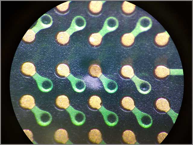
The PCB vias have parasitic inductance and capacitance, just like a PCB trace. You can calculate these values by the following formulas:
Capacitance: Cp = 1.41*ε*t*dv/(DSM‐DV)
Inductance: L= 5.08*l * [ln(4*l/DV)+1]
Where DSM is the solder mask diameter, DV is the PCB via diameter, t is the PCB thickness, PCB is relative dielectric constant, and l is the PCB via length.
These additional inductance and capacitance degrade signal integrity because of long delays and the significant rise and fall periods. It may not be an issue if you are adding PCB via in lower frequency signals designs. But it could become a critical problem in the design of high-frequency printed circuit boards.
You can decrease parasitic capacitance by choosing a PCB with a smaller dielectric constant. Or, you can also go for a thin PCB. Lastly, you can make sure that copper deposits away from the pad by increasing the solder mask area. Moreover, if you want to decrease parasitic inductance, choosing a thin PCB will do so. The equivalent inductance also reduces if you design parallels PCB via.
PCB Vias can also lead to a change in the step-function of copper trace impedance. A standard impedance drop of PCB via is around 10 %. It can change depending upon PCB thickness, PCB via its size, etc.
Summary
In Summary, we would suggest that you avoid utilizing PCB vias and layer adjustments to prevent signal distortion if possible. It would be best not to use any PCB via high-frequency clock transmission. Get rid of unnecessary pads on PCB vias where feasible because these pads build parallel plate capacitance.
If it is not possible to keep PCB via count to zero, design them so that you get lower inductance and capacitance. If the PCB via is small, you will get lower capacitance. If they have a large diameter and short length, you will get lower inductance. It would also help if you also kept the parasitic parameters’ value low to avoid detrimental effects.
If you need high-frequency PCB manufacturing services, you can contact us, and we can provide technology, materials, and quality services. We are just an email away. Contact now to get advice.
