Contents
1. What are SMDs?
As we have stated above, Surface Mount devices are devices that are manufactured through Surface Mount Technology. Widely known as the SMT, the surface mount technology is used to mount electronic components on the SMD’s PCB’s surface. With this technology, the leads and axils lay on the PCB’s conductive tracks, where with the use of soldering iron, they are mounted on the board, and no form of drilling is done to reinforce the components.
Once employed, the SMT speeds up the production process. An SMT component is mostly smaller than its through-hole counterpart because usually, it has shorter leads or no leads whatsoever. The existence of the elements is so tiny in size. Hence, they give space as holes are not bored, and both sides are available for use.
2. Repair and Maintenance of SMD Components
To grow and stay put, we all have to maintain our bodies, and so do the SMDs. The surface-mount devices use conductive tips or hot air blowers for the removal and replacement of electronic components.
Soldering iron tip attachment is a conductive tool that comes at a pocket-friendly price. The tips are in different shapes, sizes, and configurations for various SMT components and through-hole components. Composite tips are slightly at a higher cost than the soldering iron tip attachments that have heating elements.
The Hot Air SMD rework stations are more expensive than the latter two. They use nozzles of different types and sizes. The hot air repair tooling is a standard tool mainly because it is ideal for damage-free repair. An example of a perfect solution for surface mount technology components is the GOOT GSR-302.
3. Choosing Repair Equipment for SMDs
Repair systems are readily available in the market, but electronic companies need to keep in mind that repair tools don’t need to be expensive when choosing the right repair equipment.
If you need to repair many boards, you should avoid the automated repair equipment and opt for the SMT inspection equipment. Though the inspection tools are still in the developing stages, x-ray and laser inspection are the only available automated inspection equipment in the market.
Most electronic companies worldwide depend on visual inspection at 2 to 10X using a microscope or magnifying lamp.
4. Identification of SMDs
4.1. INDUCTORS
These are simply metal conductors looped through a ferrite bead and are just as similar to the through-hole designs, but instead, they have axials and caps instead of leads. They have a dark grey color and also have magnetic features.
4.2. DISCRETE SEMICONDUCTORS
They often have two or three symbol codes such as diodes and transistors because their size does not facilitate them to be marked by average numbers as other more prominent components.
4.3. INTEGRATED CIRCUITS
They are generally large enough to be imprinted with the complete part number, including the manufacturer’s specific prefix.
5. Advantages of Surface Mount Technology
Surface Mount Technology allows smaller SMD PCB designs by enabling components to be placed together on the board leading to more lightweight device designation.
1. The SMT parts are often less costly than the comparable through-hole parts. The components are replaceable on both sides of the circuit board in higher density.
2. The SMT process is faster than through-hole technology because it does not necessarily require the circuit board for assembly, making its initial costs cheaper.
3. It reduces the unwanted effects of RF, which is the Radio Frequency, by lowering resistance and induction at the connection.
4. It has a smaller radiation loop area due to its compact package, and lower lead induction has better Electromagnetic Compatibility.
5. Allows multitasking by combining high-end components.
6. PCBs created with the SMT process provide higher circuit speeds because they are more compact, leading to many manufacturers opting for this method.
7. Surface Mount Technology provides stability and better mechanical performance under conditions like shaking and vibration.
5.1. Limitations to Surface Mount Technology
As much as the Surface Mount technology is excellent for SMD devices, we can tell that it has its drawbacks. To get a clear glimpse of what we are talking about, let’s explore some of the demerits.
1. The surface mount technology components are quite small in size, making it challenging to repair them once any damage occurs.
2. There is no assurance that the solder connections can withstand the compounds used during potting application. The links may undergo damage when going through thermal cycling.
3. The soldiers can also be destroyed and weakened by mechanical stress.
4. With components that generate too much heat on their PCBs, the mounting soldering iron can melt off, rendering the whole device faulty.

6. Alternatives to SMD Technology
Although Surface mount technology is widely used and highly preferred, there are other alternatives such as the through-hole printed circuit board and the solderless breadboard technology that has been used for a variety of electronic devices.
6.1. Through-Hole PCB Design
Through-hole technology is a technique that uses the ideology of mounting the leads of electronic components onto the PCB by drilling through the circuit board. These components are inserted into holes drilled on the printed circuit boards and soldered to pads on opposite sides. They provide a stronger mechanical bond and are suitable for test and prototyping.
6.2. Pin Grid Array
Often abbreviated as PGA, the pin grid technology works the same as through-hole technology. Pins form a rectangular or square array then mounted to the PCB via the surface mount technology. These pins are later inserted into a socket and do not need to be soldered onto.
6.3. Solderless Breadboard
A Breadboard facilitates the building and testing of circuits before finalizing any circuit design. They are easy to change, as they are easily removable and adjustable. Most electronic manufacturers do not prefer this method because they do not have enough proper tools to design circuits with high voltage. It also jeopardizes your signal integrity when dealing with frequencies in the higher.
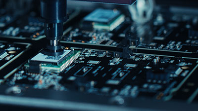
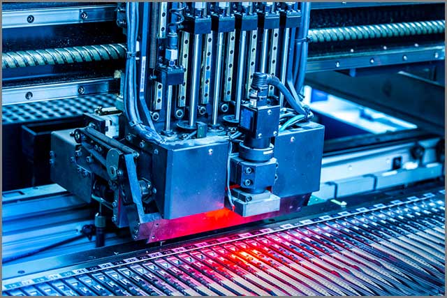
7. SMD Soldering
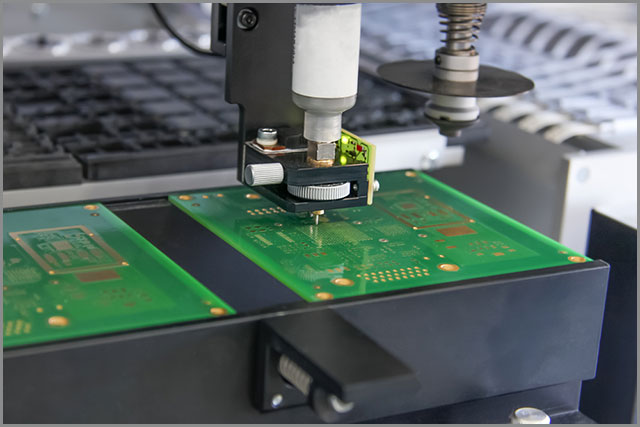
SMD soldering process
Historically speaking, we soldered SMDs by hand until the advent of pick-and-place machines. Because of their nature, SMD components are conducive to soldering.
They are perfect for first-time hobbyists who want to learn how to solder components to their PCBs. You can solder them traditionally, use solder paste, or flood them with solder.
If machines do the soldering, the first machine in the process will be the solder paste printer. It applies the solder to the pad. After the solder is applied, we perform an inspection.
Next, we surface mount the components into the PCB pads. The PCB then goes through pre-reflow automated optical inspection where we ensure the integrity of the component placement process.
Next, the PCB will go through the reflow soldering machine where we form the connections between the components and the PCB. Finally, the PCB will go through post-reflow automated optical inspection.
8. SMD vs. SMT
SMD and SMT are two terms that people sometimes erroneously use interchangeably. While the two terms are related, they are not the same thing. Once again, SMD stands for Surface Mount Device, and SMT stands for Surface Mount Technology. SMD describes the type of component, while SMT describes how we place it on the PCB. SMT decreases manufacturing costs. It also saves space and time.
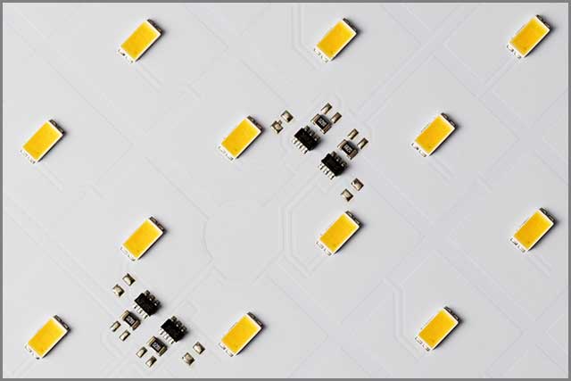
9. SMD LED
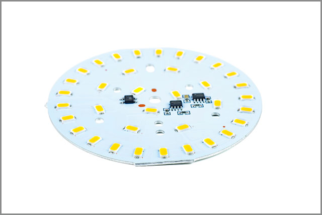
High-power SMD white lighting LED assembly
SMDs are distinct because of their lack of wires. As with other SMD components, they have solder-able metallic contacts. SMD technology makes multi-color encapsulation possible. These types of LEDs will usually feature three colors (red, green, and blue).
You can also find SMD LEDs as top-emitting chips, right-angle chips, sub-miniature chips, and reverse-mount chips.
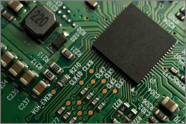
10. SMD PCB
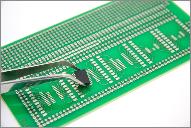
SMD component chip for PCB
A common feature of surface mount technology includes an absence of leads on components. However, sometimes these leads may be short. The main body of SMD components meets the PCB and solder joint on the same side. This makes for a seamless and easy connection.
Conclusion
Surface Mount Technology is instrumental and useful in the fabrication of electronic circuits on the Printed Circuit Board [PCB]. This design facilitates the production of better and easy-to-manufacture devices. SMDs are among the world’s most commonly used devices ranging from new generations of computers to phones and air conditioning devices, to name a few.
So whenever you need one SMD PCB for your electronic devices, reach out to our sales team and be assured of world-class services from us!


