Contents
- 1 What is PCB Assembly?
- 2 How to Prepare for PCB Assembly
- 3 PCB Assembly Process: Detailed Steps
- 4 Component Package Types in PCB Assembly
- 5 Testing and Quality Assurance in PCB Assembly
- 6 Cost Structure and Optimization in PCB Assembly
- 7 What Are Common Problems in PCB Assembly and How to Solve Them?
- 8 Future Trends in PCB Assembly
- 9 Conclusion
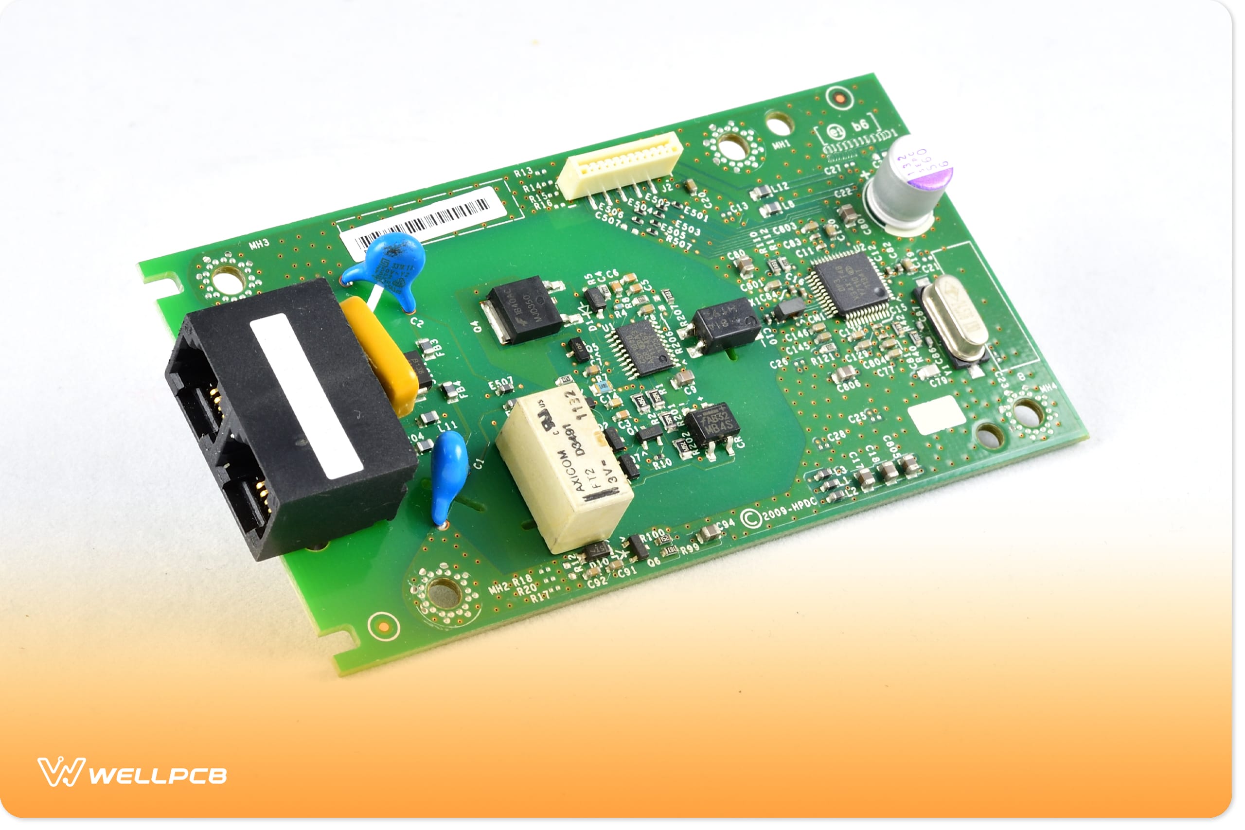
What is PCB Assembly?
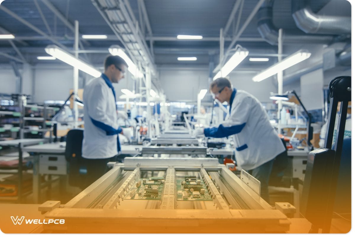
PCBA is distinct from PCB manufacturing, though the two processes are closely linked.
While circuit board manufacturing focuses on fabricating the board itself—with traces, vias, and holes—PCBA involves mounting electronic components onto the manufactured board.
Each process follows different standards and requirements to ensure a functional final product. Understanding both stages is essential for achieving a high-quality, reliable circuit board.
Key steps in the PCB assembly process include:
- Applying solder paste to the designated areas of the board
- Placing components onto the solder-paste spots
- Reflowing solder to secure the components in place
- Inspecting, testing, and conducting quality control to ensure the assembly meets standards
- Cleaning the board to remove any residue or contaminants
- Repairing and reworking any identified defects
- Applying a conformal coating to protect the assembled board
How to Prepare for PCB Assembly
PCB Assembly Requirements
Before entering the assembly phase, a manufactured PCB must have a solder mask. This mask, applied over the conductive layer, protects the board from oxidation and prevents solder bridges between closely spaced pads, while also giving the board its characteristic green color.
The essential components and equipment for PCB assembly include:
- Electronic circuit board components
- Solder flux
- Soldering machinery and equipment
- Reflow oven
- Wave soldering machine
- Pick-and-place machinery
- Inspection and testing equipment
Choosing the Right Installation Technology
There are three main installation technologies for PCB assembly:
- Surface mount technology (SMT): In this method, electrical components are mounted directly onto the surface of the PCB. These components are known as surface-mount devices (SMD).
- (Plated) through-hole technology (THT/PTH): This approach involves attaching components with leads that pass through drilled holes in the PCB. The leads are then soldered to pads on the opposite side of the board.
- Hybrid technology: A combination of SMT and THT techniques, this method utilizes both surface-mounted and through-hole components.
Design for Manufacturing (DFM) Inspection
Design for Manufacturing (DFM) ensures that products are optimized for ease of manufacturing, reducing production costs. DFM inspection assesses whether a PCB design is functional and manufacturable. It involves reviewing the bill of materials, identifying parts not recommended for production, and flagging components that require replacement.
Key benefits of DFM inspection include:
- Evaluating the product’s reproducibility and repeatability
- Providing guidance on manufacturing tolerances
- Identifying potential design issues before assembly
The inspection covers a range of factors, such as:
- Component spacing and footprint accuracy
- Component-to-edge clearance
- Polarity markings and first pin indications
- Diode cathode marks
Addressing these aspects early on helps to resolve issues like tolerance concerns and non-conformances, preventing costly mistakes during the assembly process.
PCB Assembly Process: Detailed Steps
1. Solder Paste Application
The first step in the SMT assembly process is applying solder paste using a solder paste printer. The printer applies solder to the PCB through stencil apertures, similar to how a silkscreen is used in t-shirt printing.
A mechanical fixture holds the stencil over the board, while an applicator distributes the solder across the open areas where SMT components will be mounted. For double-sided PCBs, the process is repeated on the other side.
The solder paste is a grayish mixture of powdered metal solder and flux, which gives it adhesive properties to hold components in place. Its composition typically includes copper, tin, and silver, adjusted according to the application and requirements. After application, engineers inspect the board to ensure the solder is correctly placed and in the right amount.
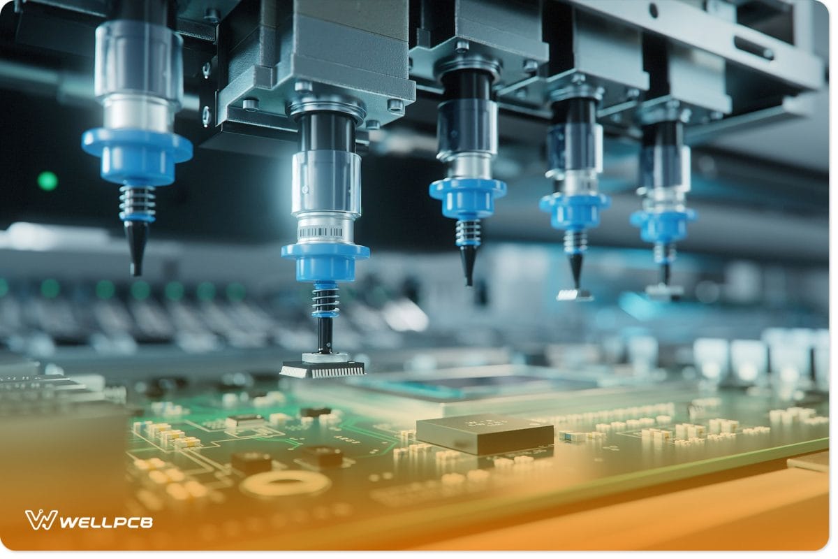
2. Pick and Place Process
SMDs lack the leads used in through-hole components and are soldered directly onto the PCB. They are the most common non-connector PCBA components.
In the past, engineers had to manually place each component using tweezers, which was a strenuous and time-consuming process. Modern pick-and-place machines automate this task, using a vacuum to pick up components and position them on the PCB’s designated coordinates.
For double-sided PCBs, pick and place is performed one side at a time, ensuring greater accuracy and consistency than manual methods. This approach also enables efficient mass production, as machines can operate continuously without fatigue.
Technology has made component placement quick and easy—all you need to do is program the machines to ensure all SMDs are placed correctly.
3. Reflow Soldering
The next step is to secure SMDs to the pads in a process known as ‘reflow soldering’, which involves heating and solidifying the solder.
The PCBs are carried along a conveyor belt through an industrial oven heated to around 480°F (250°C), causing the solder to melt. As the PCBs proceed through the oven, a series of cooling stages solidify the molten solder, permanently attaching the SMDs on the pads.
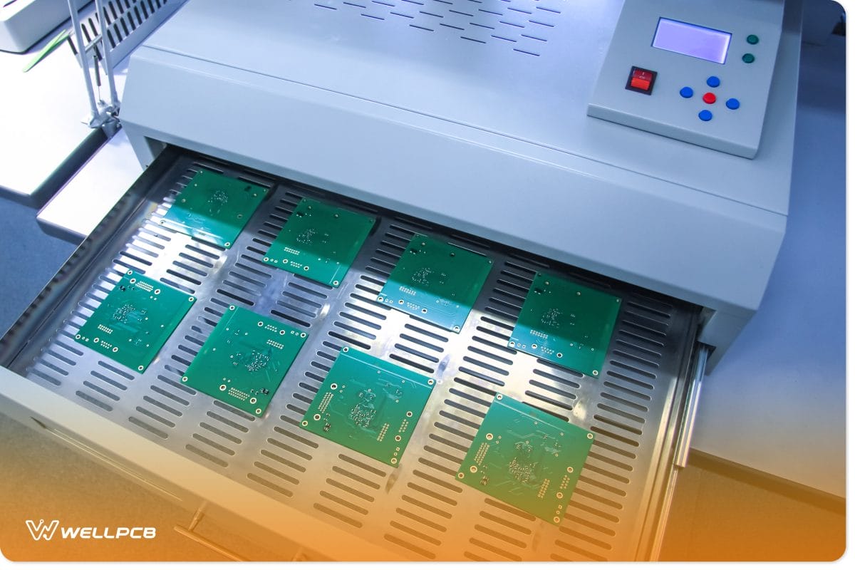
This method involves higher temperatures than manual or wave soldering, but modern SMDs are designed to withstand these conditions. Note that reflow soldering is generally unsuitable for many through-hole components due to this level of heat, so those must be attached using wave or manual soldering.
For double-sided PCBs, reflowing must be done separately for each side, starting with the one that has fewer components.
4. Through-Hole Assembly
In through-hole assembly, the manufacturer first drills plated holes for component leads and inserts components. The connections are then completed using wave soldering, where the PCB passes over a flow of molten solder, bonding it to the exposed metal areas.
Alternatively, assemblers can manually solder the components onto the PCB using a soldering iron. This is often used for small-scale productions or those requiring high degrees of accuracy. Manual soldering can be time-consuming, however, so many companies avoid relying on it.
Once the assembler completes the soldering process, the PCB is cleaned to remove residual solder flux and contaminants that could cause corrosion.
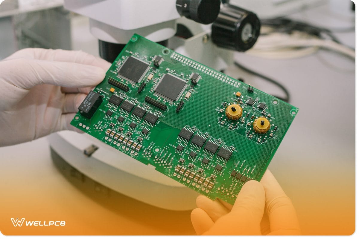
5. Inspection and Quality Control
Manual inspection is often unreliable, so modern PCB assembly typically uses machine-controlled methods such as Automatic Optical Inspection (AOI). Such automated techniques are more suitable for large batches, as they can rapidly process a high volume PCB.
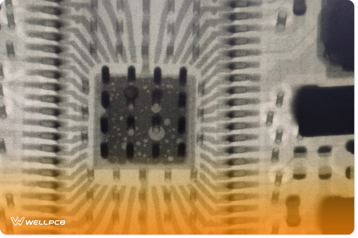
While less common, X-ray inspection is an alternative approach that’s employed for complex, multi-layered PCBs. This is because it allows for visualization of hidden issues within the layers.
Component Package Types in PCB Assembly
There’s an SMT variant for every THT component. As previously mentioned, we refer to SMT components as Surface Mount Devices (SMDs). Here are the most common SMDs and package types used in PCB assembly:
Surface mount devices (SMDs)
The most common SMDs include:
- Resistors: Allows circuit boards to regulate the flow of current. Each resistor has a printed code on its encasement denoting its size. For instance, 0402 indicates that an SMD resistor has a package length of 0.04 inches and a width of 0.02 inches.
- Capacitors: These store and release electric energy. Circuit boards use capacitors to filter out electric noise, deal with voltage drops, or provide bursts of energy to components. Capacitors are categorized according to their materials, the most common being ceramic, electrolytic, and tantalum.
- Inductors: Maintain current flow by storing energy in a magnetic field.
- Diodes: Enable current rectification.
- Transistors: Facilitate electrical switching and signal amplification.
- Integrated circuits (ICs): Contain miniaturized electronic circuits within a single package.
SMT has revolutionized IC assembly, with Ball Grid Arrays (BGAs) and Quad Flat No-Lead (QFN) packages being two of the most important types.
Ball Grid Array (BGA)
BGAs evolved from pin grid arrays (PGAs), replacing pins with tiny solder balls arranged in a grid. During assembly, these solder balls are positioned on the board and heated in a specialized oven, where surface tension keeps the components in place.
Advantages of BGA packages include:
- Higher connection density in a compact area.
- Enhanced heat dissipation.
- Superior electrical performance.
- Lightweight and cost-effective design.
As such, BGAs have become a popular technique used in manufacturing integrated circuits and electronic devices.
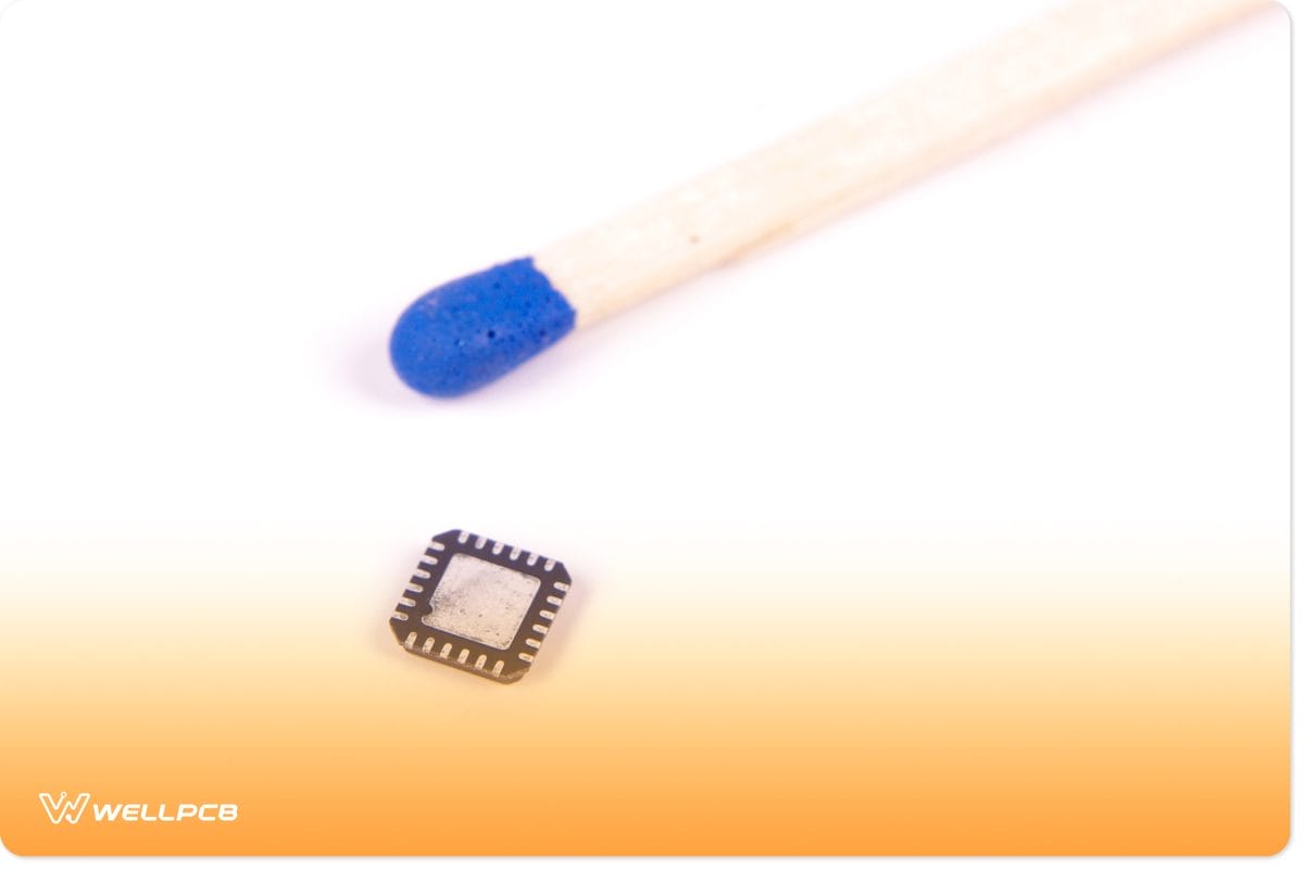
Quad Flat No-Lead (QFN) Packages
The QFN package is popular for its outstanding electrical performance, cost efficiency, and small profile. It connects integrated circuits (ICs) to SMT-based PCB assemblies and is often considered a type of chip scale package (CSP) due to its exposed pads and compact form factor.
QFNs can have one of two pin configuration types:
- Single-row: A single row of pins near the package edges, ideal for assemblies where the conservation of space is important.
- Dual/multi-row: Multiple rows of pins for higher pin counts, enabling denser, more reliable connections.
Regardless of the configuration, QFN packages offer significant benefits for PCB assemblies due to their compact size and lightweight design. These features make them ideal for space-constrained applications, such as those found in Internet-of-Things (IoT) devices.
The short pins of QFN packages help to minimize inductance and noise, thereby improving digital signal integrity. Additionally, QFN packages often include exposed thermal pads on the underside, which enhance heat dissipation and make thermal management more efficient.
Hybrid and Specialized Components
In addition to QFN and BGA, manufacturers have various hybrid and specialized packaging options to choose from, each designed for specific use cases:
- System-in-package (SiP): Combines multiple ICs and passive components within a single hybrid package, significantly reducing board size. SiP is commonly found in compact devices like smartphones, where space is at a premium.
- Multi-chip modules (MCM): Integrates multiple ICs, each serving a different function, into a single package. This design reduces interconnect delays and enhances overall performance. MCMs are commonly used in high-performance applications such as aerospace, advanced computing, and telecommunications.
- Leadless chip carrier (LCC): Instead of conventional leads, these packages have solder bumps underneath their encasements. This enables them to form high-density connections. They also offer excellent heat management and electrical performance, making them suitable for demanding environments.
- Chip-on-board (COB): Involves directly mounting an exposed die onto the PCB and wire-bonding it. The COB approach is space-efficient, cost-effective, and offers outstanding thermal performance. It is widely used in applications like LED lighting, displays, and sensors.
- Wafer-level chip scale package (WLCSP): The die is packaged at the wafer level, resulting in a package that is nearly identical in size to the die itself. This provides the smallest possible footprint and excellent electrical performance, ideal for miniaturized applications.
- Flip-chip package: Commonly found in graphics processing units (GPUs) and high-speed communication devices, this package involves flipping the die and bonding it to the substrate using solder bumps. The flip-chip design optimizes performance for high-frequency and high-power applications.
Testing and Quality Assurance in PCB Assembly
Ensuring that your PCBs function as intended is crucial, as failures can be costly and damaging to a company’s reputation. Testing helps prevent defects and recalls, reduces costs, saves time, and ensures the reliability and quality of the assembled PCBs. Testing methods can be divided into common and advanced techniques.
Common Testing Methods
- Visual inspection: An operator manually checks the PCBA for visible defects, such as solder joint issues, component misalignment, or physical damage. This method is typically used as part of a multi-stage inspection process to identify flaws early.
- In-circuit testing (ICT): Isolates and tests each component individually to detect connection issues like shorts and opens. ICT uses automated equipment for reliability, speed, and accuracy, making it ideal for identifying specific defects.
- Functional circuit testing (FCT): Evaluates the board’s performance under real-world conditions by simulating practical scenarios and applying stress tests. It serves as the final checkpoint to ensure the PCBA functions correctly before deployment.
Advanced Testing Techniques
- X-ray inspection (AXI): Utilizes X-rays to generate a transparent image revealing the topography and structure of the PCB. It can help identify any hidden defects that escape other tests. X-ray inspection is particularly useful in finding connection and solder-based faults in multi-layer PCBs.
- Boundary scan/JTAG testing: Assesses the integrity of PCB and IC connections by driving signals through the IC and recording the state of its pins. Boundary testing grants access to the PCB/IC’s internal nodes, enabling manufacturers to observe and access the various signal points and paths in the device.
Cost Structure and Optimization in PCB Assembly
Several factors affect the cost of PCB assembly, including:
- Labor costs: Wages for the workforce directly affect the final costs of the PCB.
- Turnaround time: Faster assembly and delivery times will increase costs, especially if the manufacturer is asked to prioritize your order.
- Quantity: Costs scale with the number of units produced; larger orders cost more overall, though economies of scale can reduce per-unit costs.
- Technology: Advanced equipment can be more expensive to operate, but may also offer greater efficiency and higher-quality results.
- Material selection: Cost will depend on the type of materials and components your design requires. For instance, fire-resistant and high-performance materials tend to cost more. The amount of each material your board needs will also affect cost.
- Insertion technology: The scale of your production will determine whether SMT or THT is more cost-effective. SMT is best for high-volume assemblies, while THT is better suited for small-scale projects.
Strategies for Cost Reduction
If you want to reduce the costs of PCB assembly, there are several measures you can take:
- Provide complete bills of material (BOMs): Ensure accurate and detailed BOMs are delivered to the manufacturer.
- Use sourcing services: Take advantage of the manufacturer’s component sourcing capabilities to reduce material costs.
- Prioritize inspection: Thorough inspection will help prevent costly rework or recalls.
- Optimize board schematics: Streamline designs to reduce complexity and material usage, which will help minimize overall costs.
What Are Common Problems in PCB Assembly and How to Solve Them?
Given its complexity, various issues can arise throughout the PCB assembly process. Here are some of the most common problems and their solutions:
- Solder joint defects: Issues like solder bridging and cold joints are common, especially in SMT assembly. To avoid these, apply the correct amount of solder and use Automatic Optical Inspection (AOI) to detect defects early. Manufacturers should also ensure enough heat during reflow and that the pads are prepared correctly.
- Incorrect component placement: Components may be positioned on the wrong pads due to human error or pick-and-place programming issues. To ensure accurate placement, always implement thorough quality control, including peer-reviewed inspections and AOI, and mark all components clearly.
- Component shifting: Components may unintentionally move during the reflow process. A suboptimal reflow profile is usually the culprit in such cases. To prevent this, manufacturers must use the correct reflow profile and ensure that the PCB is stable during the soldering process. They should also verify the placement accuracy using AOI.
- Delamination: Exposure to heat and moisture may cause the PCB substrate to separate. Manufacturers can prevent this by preheating or baking the PCB to reduce moisture, carefully managing the reflow temperature, and by using high-quality materials that won’t fray easily.
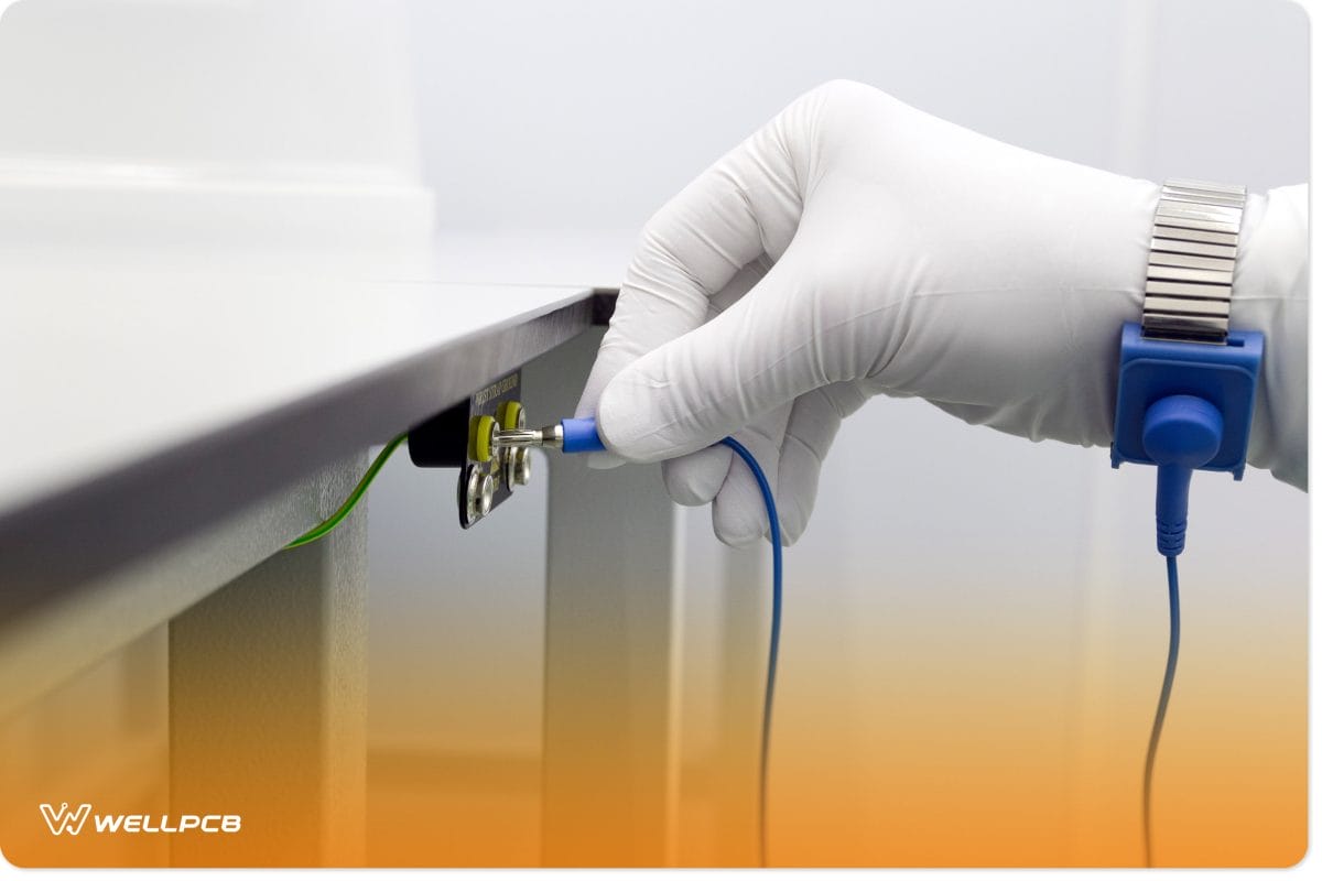
- Electrostatic discharge (ESD) damage: Sensitive components can be damaged by static electricity during handling. You can minimize this risk by using anti-static equipment like gloves, mats, and bracelets and by ensuring workstations are properly grounded.
Future Trends in PCB Assembly
As previously mentioned, insertion technologies like SMT help automate and optimize the PCB assembly process. While improving speed and accuracy, it isn’t perfect and there’s still room for further optimization. Emerging technologies such as Artificial Intelligence (AI) and the Industrial Internet of Things (IIoT) are set to push PCB assembly to new levels of automation and efficiency.
These technologies may allow supervisors to remotely view and manage multiple assemblies simultaneously, potentially reducing the need for a large human workforce. This not only lowers costs but also minimizes risks in hazardous environments. AI, on the other hand, can help identify the best suppliers for components and predict supply chain disruptions.
AI-powered X-ray inspection can potentially find flaws and defects, without the need for human intervention and supervision. Such advancements can lead to fully automated assembly lines—making the PCB assembly processes faster, more reliable, and more cost-effective.
These technologies can also enable more sustainable manufacturing practices. Current soldering and reflow processes take a huge toll on the environment, as they use a substantial amount of energy and generate significant heat. AI can help us implement more precise temperature control and optimize the overall soldering process.
Conclusion
PCB assembly is a complex process with multiple stages that are essential for ensuring the durability and functionality of the final PCB. This guide has provided a comprehensive window into the world of PCB assembly, covering key stages, components, and packaging types, as well as strategies for overcoming common challenges. Having read this guide, you should be in a better position to assess the quality of a PCB assembler.
As with any technology-driven industry, PCB manufacturing and assembly are continually evolving. Staying informed with the latest industry advancements is crucial to maintaining a competitive edge, so be sure to visit our blog regularly.
For expert guidance and support with your next PCB project, get in touch with us today.