You can follow the following tips to make an excellent PCB Landing and Layout:

1. PCB Landing And Layout—Steps
- Troubleshooting of Components
Before arranging PCB Landing And Layout, one should consider which will be critical to investigate the circuit. If those are not efficiently open, include a test directly associated with them.
2. Formation of space amid components
The components’ spacing will streamline auto-routing and make the soldering easier. If there are other components, more space will need.
3. Put components with a related orientation
If all parts are arranged similarly, you won’t commit errors when soldering or assessing a component.
4. Print the circuit drawing to check whether the parts’ sizes coordinate
Place every piece over that layout paper to check whether they coordinate. At times datasheets might have been mistaken.
5. Trade wiring headings between layers
Drawing vertical traces at one side and the flat on the alternate encourages the wiring of those lines that need to traverse the others.
6. Select the thickness of lines relying on current
The thickness of these lines ought to be measured by the assessed current that moves through them; if the width of the line increases, the resistance decreases.
7. Maintain a strategic distance from 90 Degree points with follows
Always use two bends with a perspective of 45 degrees because sharp right-edge turns are hard to keep trace width consistent.
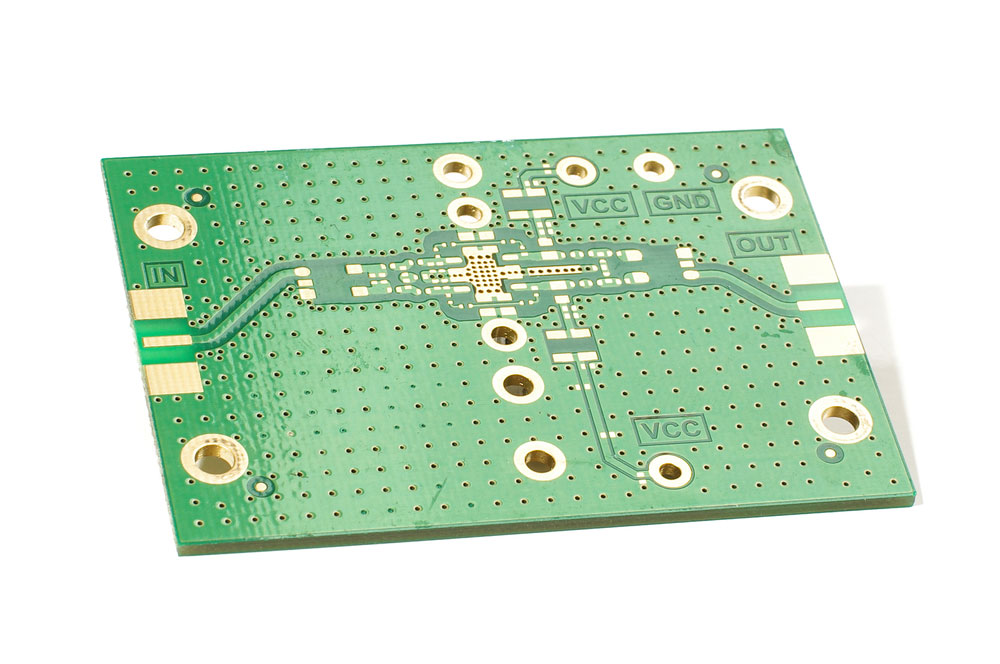
8. Utilize the silk coating
This coating is used for labeling purposes.
9. Utilize the schematic versus design examination
Match your layout with a schematic by using software tools so that error must not there.
10. Make a ground
To avoid voltage drop due to traces, you must first build a ground by filling copper.
11. Use bypass capacitors
Their use reduces AC components (ripples), noise, and unwanted signals. These are used during the construction of the power supply.
12. Course the differential flag follows in parallel
This is successful if the traces of the two signs take after comparative ways, with the goal that the disturbance aggravates the two ways similarly. Therefore the differential signal traces are routed in parallel.
13. For PCB Mounting, Always solder small components first and then go for large parts.
14. While soldering, remember that there must not be a short circuit. Also, make use of flux during soldering.
15. For the measurement of resistance, use the multimeter’s resistance-checking mode instead of the continuity test mode.


