
When hardware or firmware is built on, the manufacturers or employers ask to develop a hardware prototype.
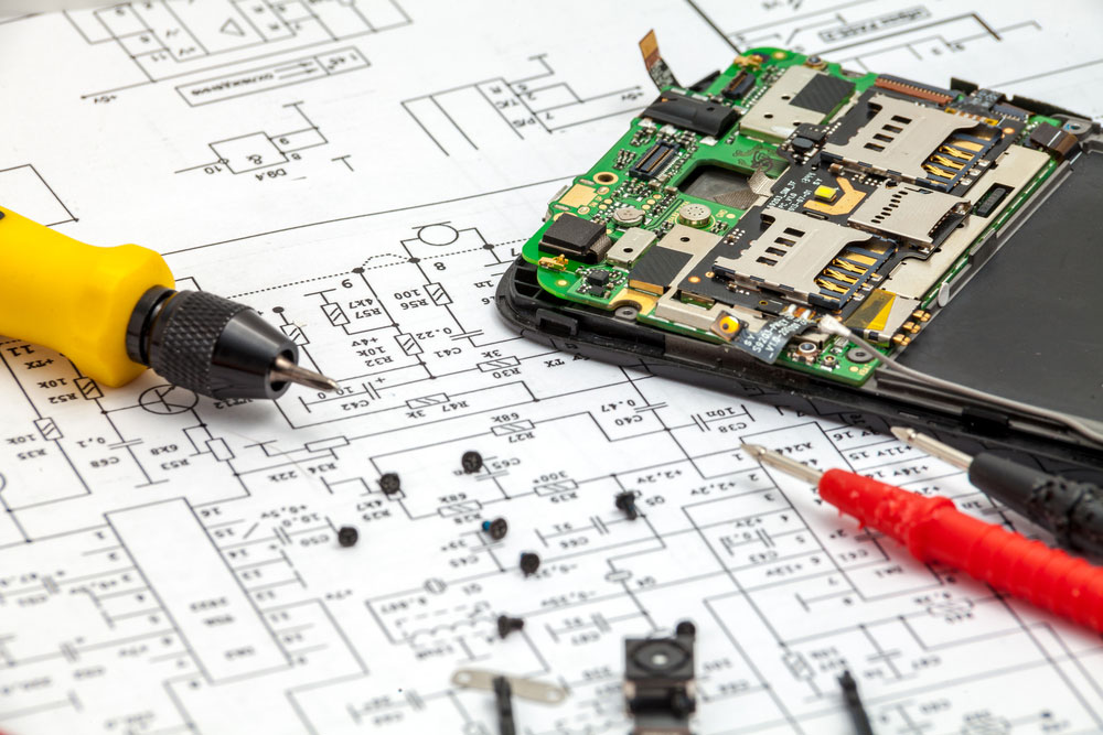
Prototype PCB, an electronic product, from idea conceiving to a finished marketable product, passes through various iterative steps like requirement specifications, circuit design, breadboarding of critical circuit sections, design reviews, etc.
This prototyping or experimental work leads to a proof of concept of that hardware.
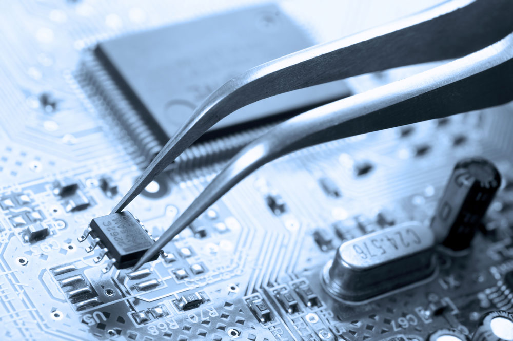
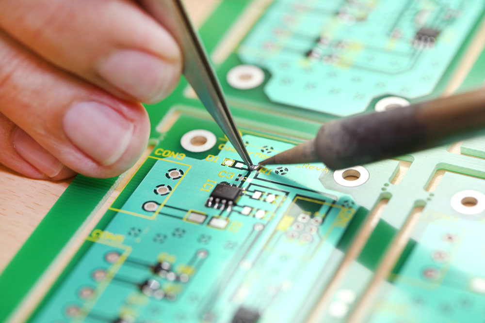
Generally, a circuit on a PCB needs enough components for functional testing and verification before it is qualified and passed for production.
1. Prototype PCB Specification and Benefit
In PCBs, the prototyping occurs significantly in earlier stages after circuit design, layout, and PCB fabrication.
The experimentation in the prototyping stage assures that the hardware meets the specifications.
The goal is to verify that the product will be functional, accurate enough as per specifications, throughput efficient, and environment-friendly when deployed in the field.
This stage may take more than one iteration if the PCB underperforms.
The benefit of prototyping is revealing and removing the shortcomings that may cause product failure if otherwise ignored.
The key points which are kept in mind during prototyping are under or over-designed circuits, which affect the functionality and cost, respectively, the overhead of assembly time and cost, practical limitations of components that are not found in simulation,
PCB dimensions, bill of material cost, placement inside the mechanical enclosure, heat dissipation, etc.
Another benefit of a prototype PCB mounted inside a prototype mechanical enclosure may be used to get user feedback.
Generally, the large production houses, only a few PCBs are manufactured for prototyping to reduce cost and manufacturing time.
This is the final PCB if it works in the first run, i.e., the same PCB goes for final production.
However, if the prototype PCB does not qualify all of the required specifications or is unacceptable, the problem is probed by conducting a detailed design review.
After the design review, a new iteration starts by making the necessary design amendments at the appropriate level, i.e., circuit design, PCB layout, PCB material selection, etc.

2. How does WellPCB do
The small or with low budget constraint setups go towards soft cost PCB fabrication either as a single layer or divided and multiple single layer PCBs (ignoring the actual dimensions) and finally interconnecting them with cable and connectors.
This method suits hobbyists, general household items, and gadgets producers. This method provides a low-cost solution to product specifications and validation.
So, WellPCB provides this service: Once the prototype is built successfully, the last iteration goes towards the final PCB with exact dimensions for final testing, which is almost the production PCB in many cases.
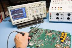
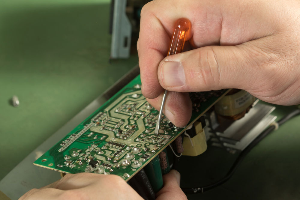
Figure: A PCB troubleshooting after manufacturing and assembling
