Contents
- 1 What are Transparent PCBs?
- 2 What are Transparent PCB Substrates?
- 3 Types of Transparent PCBs
- 4 Materials for Manufacturing Transparent PCBs
- 5 Transparent PCB Design Guidelines and Rules
- 6 Transparent PCB Manufacturing Steps
- 7 Future Trends in The Manufacturing and Usage of Transparent PCBs
- 8 Final Words
What are Transparent PCBs?

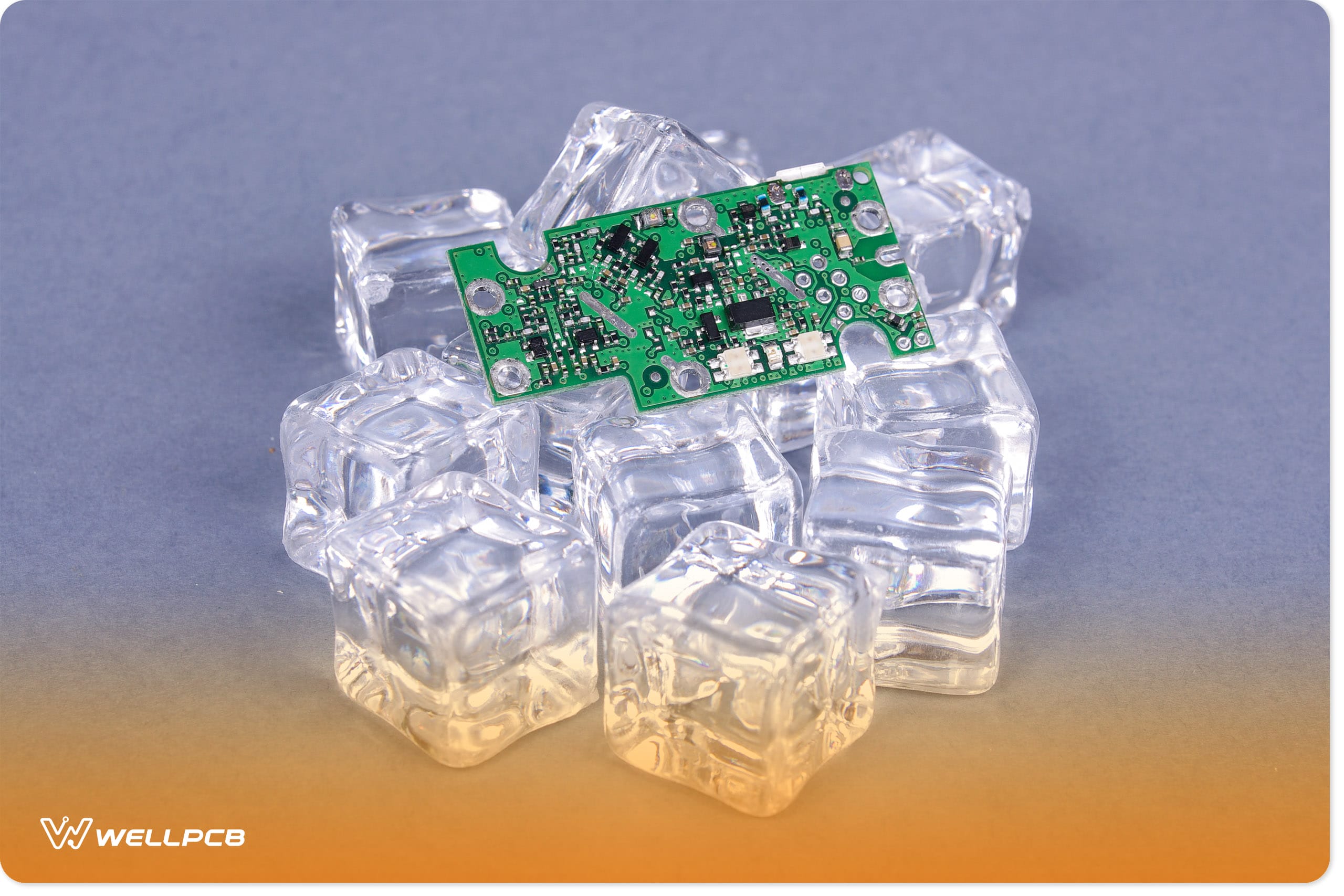
A transparent PCB
Transparent PCBs are variants of flexible PCBs offering more benefits than their flex and flex-rigid predecessors.
Undoubtedly, the innovation utilizes polyamide, making it incredibly flexible and thin.
Further, you can find these circuit boards in the automotive industry, particularly underbody controls, ABS systems, instrument panels, and other components.
In addition, the computer peripherals industry also utilizes transparent PCBs to connect printers to hard disk drives.
Moreover, consumer electronics can also use transparent PCBs.
Usually, you’ll find them in devices like training monitors, cameras, calculators, and mobile phones.
What are Transparent PCB Substrates?
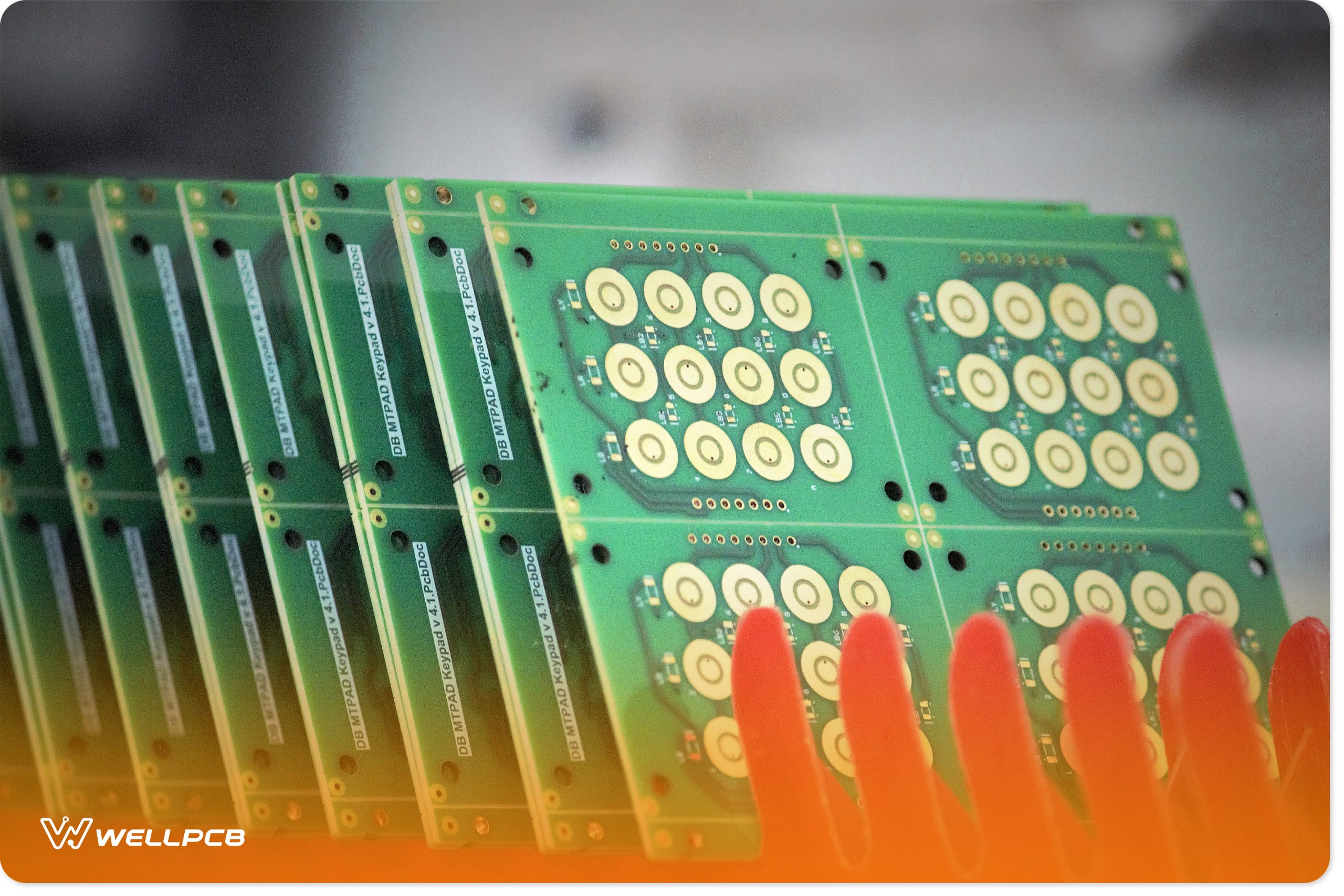
Transparent keyboard PCB
Currently, you can use two substrates for transparent PCBs, including ceramics and glass.
PCB variants with ceramic materials provide excellent thermal conductivity that’s better compared to glass models.
However, transparent PCBs with glass substrates provide enhanced optical transmissivity.
Interestingly, ceramic substrates offer 75% to 80% transmissivity, while glass variants possess up to 99.5% to 99.99%.
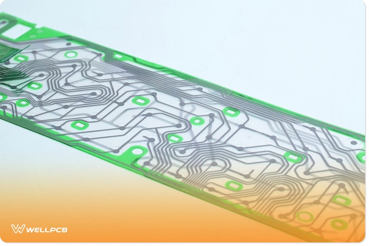
Types of Transparent PCBs
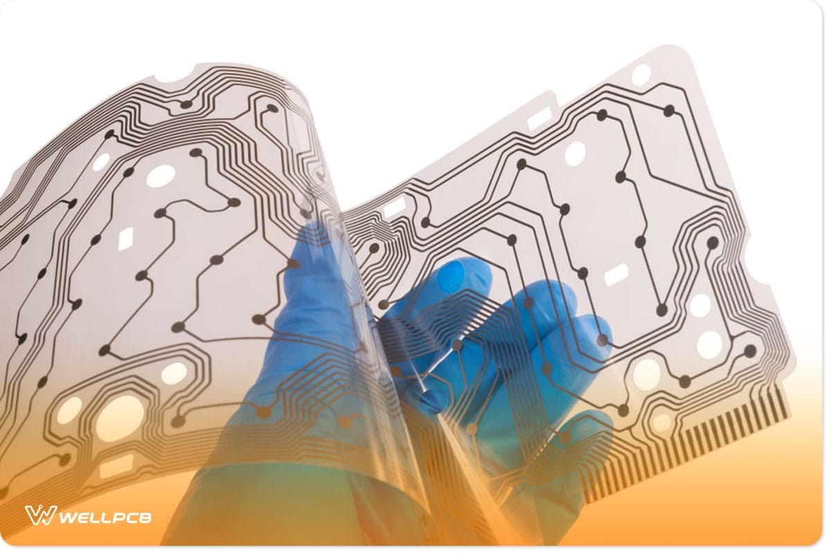
A hand folding a transparent PCB
As mentioned earlier, we have two substrates used for making these PCBs, which translates to two types: Glass and Ceramic transparent circuit boards.
So, let’s take a deeper look at these models.
Note: We also have transparent flexible PCBs, which we’ll discuss in this section.
Glass Transparent PCBs
Transparent PCB on a table
Usually, manufacturers produce the glass substrate from a blend of limestone, sand, soda, and ash. Thankfully, these materials are recyclable and eco-friendly.
Further, tempered glass is the most widespread variant of this substrate.
Typically, manufacturers pre-stress and reprocess the glass to achieve high durability.
Additionally, tempered glass transparent PCBs can absorb impact force and shock.
Also, sapphire glass substrates provide the most rigid and durable models of all glass PCBs.
Therefore, you can find them in high-end electronic equipment due to their enhanced thermal properties and dielectrics.
In short, PCBs made from sapphire glass substrates work in devices built for space and satellites.
And transparent PCBs made from glass substrates can transmit light omnidirectional.
Hence, you can reflect light via the circuit board from almost all angles.
Benefits of Glass Transparent PCBs
You can get the following benefits from transparent glass PCBs:
- Incredible resistance to wear and tear.
- Glass transparent PCBs offer maximum transparency.
- They’re resistant to heat and deformation.
- These PCBs provide an incredibly flat surface.
But it’s crucial to note that glass transparent PCBs placed under extreme heat for extended periods will deform at trickling speed.
As a result, these variants are one of the most desirable variants.
In truth, glass substrates can withstand up to 1000°C, and their materials are simple to source, making them easy to produce.
Lastly, glass transparent PCBs are significantly less expensive than their ceramic counterparts.
Drawbacks
While the glass PCB substrate offers maximum transparency, the copper traces will remain visible.
However, manufacturers are working towards innovations to fix such issues for true transparency.
Ceramic Transparent PCBs
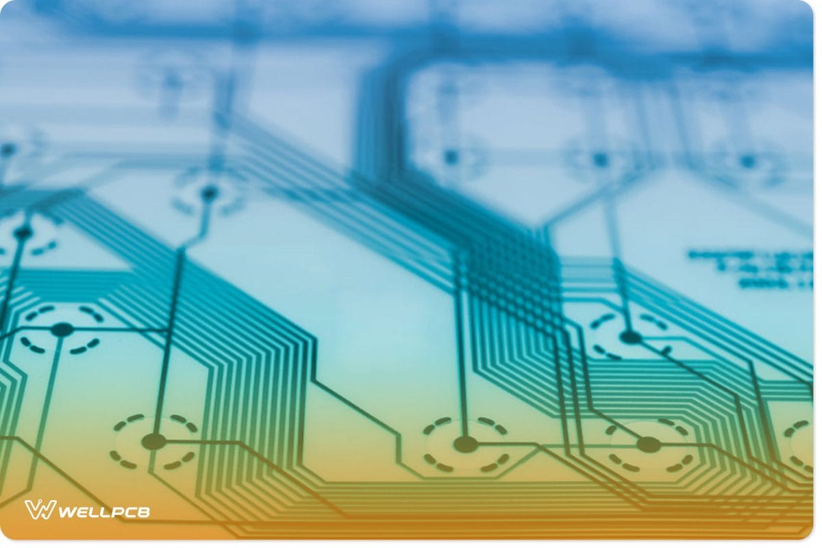
Transparent PCB
Typically, transparent ceramic PCBs feature mixtures of materials like Aron, magnesium oxide, Al-Mg spinel, Yttrium oxide, and alumina.
For example, these circuit boards can have fine alumina powder at small levels, like 5 – 10%. In addition, this process shoots the hardness values from 6H to 8H.
Also, some manufacturers may use oil-based alumina liquid, while others utilize water-based alumina liquid to produce transparent PCBs.
However, most of these boards use glass-based solder masks to achieve better transparency.
Advantages of Ceramic Transparent PCBs
Here are some pros of using transparent ceramic variants.
- Ceramic transparent PCBs provide various optical features.
- These circuit boards offer enhanced electrical insulation.
- Ceramic boards feature over 24 – 31.4 W/mk thermal conductivity.
- The boards absorb water at slow rates.
- These boards can resist high temperatures.
- Lastly, they have a low and stable coefficient of thermal expansion.
Applications
You can use ceramic transparent PCBs in optical sensors, infrared missile windows, high-pressure sodium vapor lamps, aircraft, and high-power LEDs.
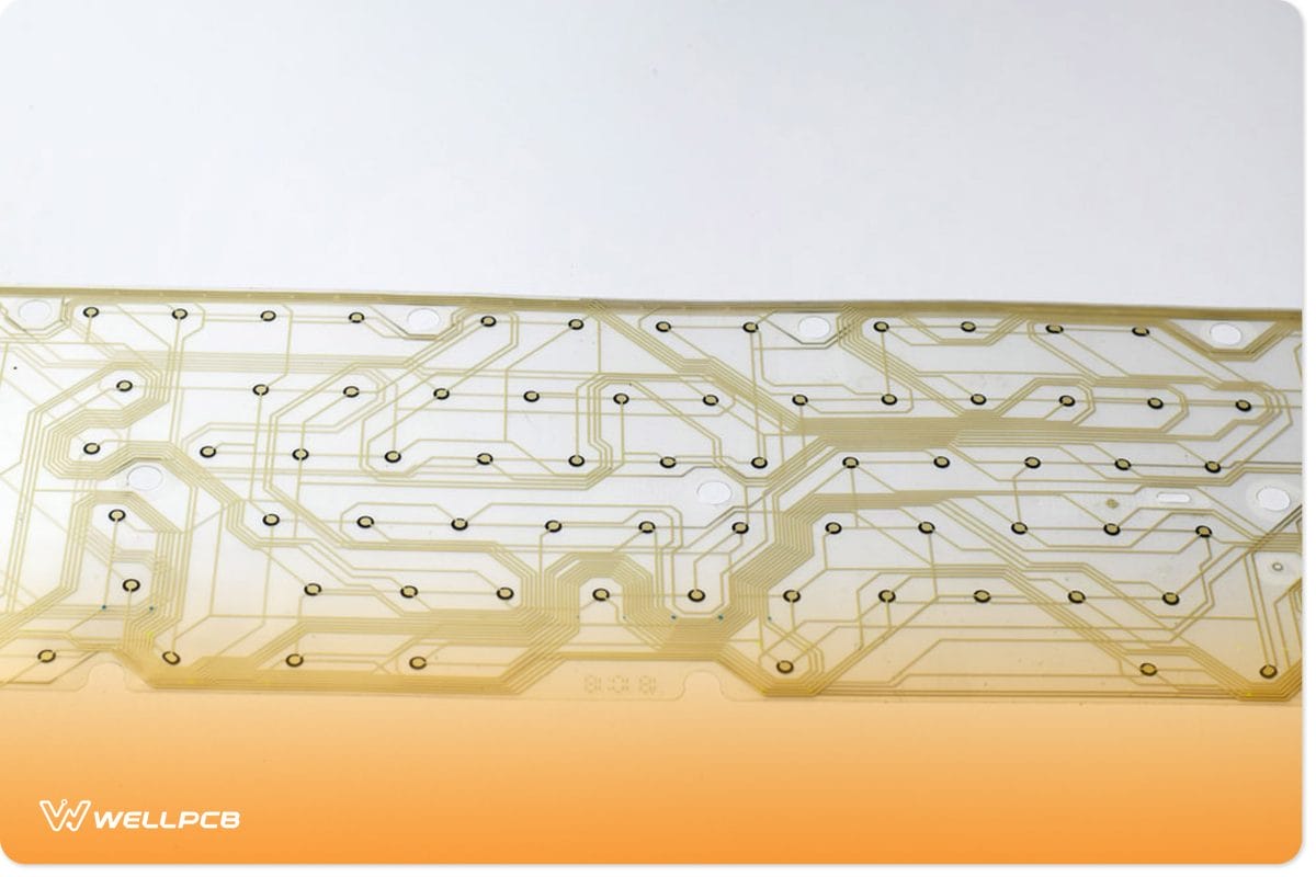
Transparent Flexible PCBs
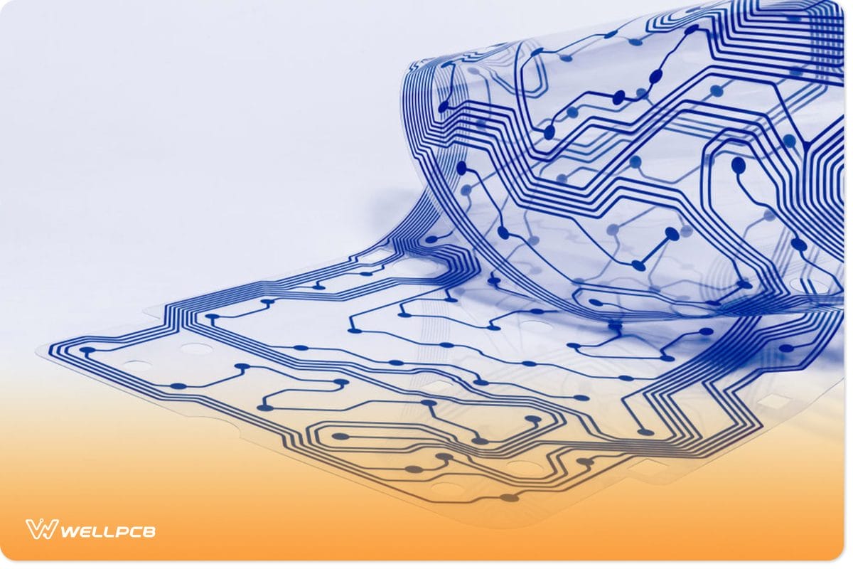
Flexible transparent PCB
PCB manufacturers can combine transparency and flexibility into one board by utilizing thin PET films.
In addition, they can manufacture these circuit boards in various colors like light green, blue, white, etc.
Interestingly, these transparent PET materials can produce flexible PCBs with different benefits from regular variants.
Also, some innovative methods can make the board’s conductive traces equally transparent.
To achieve this, the fabricator can clamp the board with visible conductive traces between two PET films, protecting and making the PCB invisible.
Pros of Using Transparent Flexible PCBs
- Transparent flexible PCBs offer numerous optical features.
- They can cut down weight and form factors. Also, transparent flexible PCBs can initiate product miniaturization.
- Unlike standard rigid PCBs, these boards can reduce overall weight by over 90%.
- You can twist, fold, move, and bend these PCBs as much as you like without damage.
- These PCBs offer stable dimensions.
Applications
Here’s a list of things you can do with flexible transparent PCBs:
- Instrument panels
- Smart contact lenses
- Automatic control systems
- Mobile phones
- Electronic skins
- Medical devices
- Cameras
- Electronic calculators
- ABS systems
Materials for Manufacturing Transparent PCBs
Transparent PCB on a table
Colored PCBs use materials that don’t allow light to pass through them. They commonly use a combination of flame-retardant fiberglass and resin.
Transparent PCBs require material that is translucent but is still strong and can facilitate translucence.
Of course, the material you ultimately choose will depend on the type of transparent PCB you hope to design and manufacture. Nevertheless, these are your options:
- Polyethylene Terephthalate (PET): A strong thermoplastic commonly used in water bottles, clothing and food containers.
- Polycarbonate: A transparent high-grade thermoplastic that is strong is famous for its strength and transparency. In addition to its use for rigid PCB fabrication, it’s also ideal for roof sheeting.
- Polymethyl Methacrylate (PMMA): Many commonly refer to it as acrylic glass. It is a synthetic resin and because it features high-light transmissions, manufacturers commonly use it in place of glass. It can be found in skylights, illuminated signs and shatterproof windscreens and windows.
- Liquid Crystal Polymer (LCP): These are exceptionally strong translucent materials that allow manufacturers to produce tensile, thin and flexible transparent PCBs.
- Glass Reinforced Epoxy (GRE): A glass fiber-reinforced plastic. Not only does this material’s strength and clarity lend itself well to transparent PCB manufacture but factories also utilize it in pipes, casings, fittings and gaskets. It’s cheaper than steel and easier to work with too.
Transparent PCB Design Guidelines and Rules
Before you produce your transparent PCB, there are a few guidelines and design rules you must adhere to in order to ensure a successful production. First, let’s cover the guidelines:
Transparent PCB Design Guidelines
- Make use of alignment markers to ensure accurate component placement.
- Ensure that your transparent PCB will dissipate heat effectively by implementing extensive thermal simulations.
- Select components carefully, especially visible ones, to avoid impairing the boards’ transparency. You must also place these components strategically.
- As mentioned, you must carefully consider what substrate material you’ll use for the transparent PCB. You must base your decision on how well the material dissipates heat, how strong it is, the cost and the dielectric performance.
- You must work closely with reputable and experienced PCB manufacturers who can help you correct and refine your PCB design. The PCB manufacturer should be able to help you review the design and ensure that it meets directed energy and fire resistance safety regulations.
- In addition to thermal simulation, you must consider testing your design’s electronic performance using a circuit simulator and a live prototype.
- Because transparent PCBs have lower resolutions, making them harder to inspect, it’s best to implement larger spacing between conductors. Additionally, you must ensure that these conductors fulfill your PCB’s current and voltage requirements.
- To strike a balance between transparency and visibility, consider using reverse-mount SMDs and/or components with transparent leads.
Transparent PCB Design Rules
The following design rules also apply:
- The panel dimensions of transparent flexible PCBs should not be less than 100mm (3,93 inches).
- The transparent PCB should have a conductor thickness of around 144 grams (5,1 ounces).
- The recommended board thickness for transparent PCBs is 0,38mm.
- The best surface finishes for most PCBs are ENIG and ENEPIG. This may also apply to transparent PCBs too.
- Your transparent PCB should have a standard solder resist with a minimum opening of 0.2mm.
- The transparent PCB should feature direct and concise trace lengths.
- Transparent PCBs should have 8mm of minimum line spacing between traces.
- If you intend to use the PCB for high-speed operations, you must consider adding decoupling capacitors as they will reduce noise.
- The acceptable roughness of a PCB is less than 0.5mm.
- Your transparent PCB dimension tolerance must be less than 4mm.

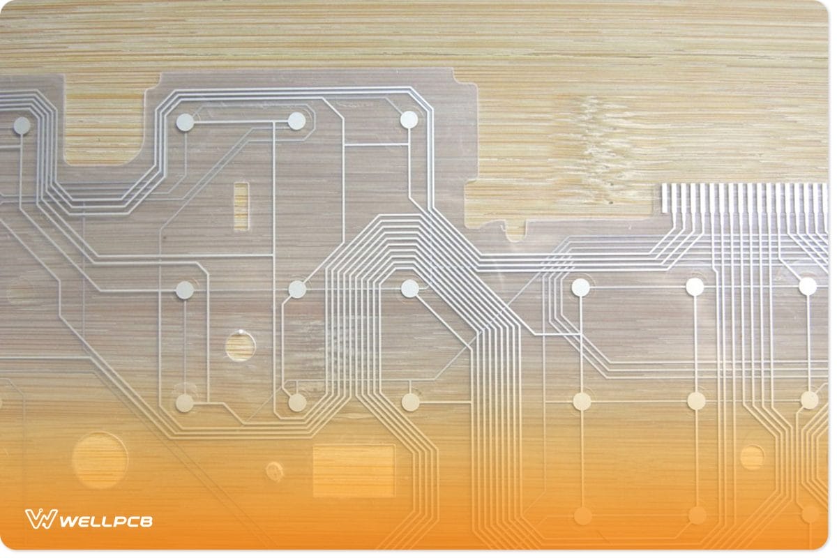
Electronic Flex Circuit Board Plastic Membrane
Transparent PCB Manufacturing Steps
The design and manufacture of transparent PCBs are not very different from the manufacture of opaque or colored PCBs.
The material selection is likely the biggest difference between the two processes.
When designing and building your transparent PCB, you must first select, source and arrange the necessary material.
Use PCB layout software to prepare the design and then print it out.
Next, assess and perform quality checks on the design and make corrections where necessary.
Once validation is complete, you can then cut and produce the substrate using your preferred transparent material.
Apply the PCB layout onto the substrate using copper foil and photoresist. Next, develop the photoresist by exposing it to light. Clean the PCB with an etching solution.
This will remove any excess copper. You can finally wash and dry your transparent PCB.
Future Trends in The Manufacturing and Usage of Transparent PCBs
As impractical as transparent may seem to some people, they’re not going away anytime soon.
We can expect to see more research and development going into discovering less expensive and more reliable materials for PCB production.
You can also expect to see innovations in manufacturing that allow for transparent PCBs with higher layer counts and smaller vias.
With the popularity of the Internet-of-Things (IoT) and the advancement of the Industrial Internet-of-Things (IIoT), we can expect to see more organizations implementing transparent PCBs.
This is because manufacturers can use Transparent PCBs to increase and highlight the visibility of components, making them easier to spot and fix.
While we’re long past the clear craze of the 90s, fully and partially translucent technology may still make a comeback.
It can potentially complement minimalist and sterile home and office decor.
Many consumers have begun to use LED-based indoor and outdoor fixtures in place of incandescent bulbs.
They can implement transparent circuit boards in place of solid ones to enhance their appearance.
More design software will be dedicated to creating effective, transparent PCB designs.
Manufacturers and designers will be able to make transparent boards that are more flexible and thinner, enabling them to fit in more compact products.
Manufacturers will also be able to implement additive processing measures such as inkjet printing of conductors.
This will make the production process cheaper and more efficient. They’ll also be able to embed touch directly on transparent boards, leading to thinner and more futuristic devices.
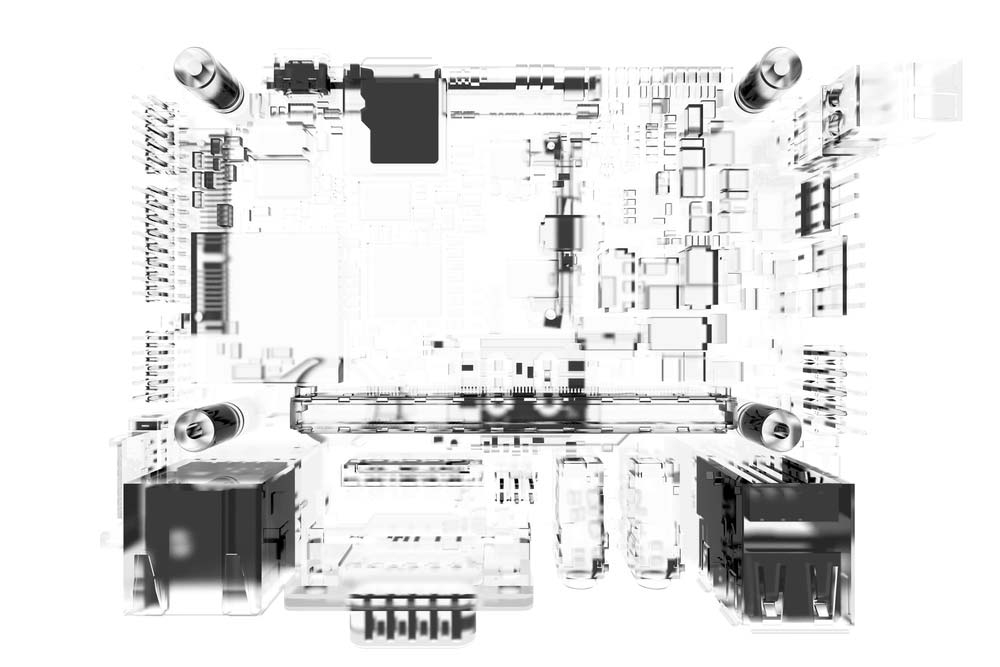
Cpu Main Board 3d Rendered White | Shutterstock
Final Words
The PCB industry is getting countless innovations, and transparent boards are among the top. Manufacturers are now employing these revolutionary changes to satisfy the requirements of various electronic devices.
In addition, transparent PCBs also support the movement toward miniature circuit boards and devices. More importantly, you can have limitless devices with transparent PCBs.
And you can find the three types of transparent PCBs mentioned, each offering unique benefits. For example, ceramic variants offer more durability, while glass ones provide more transparency. In short, flexible PCBs offer the best circuit invisibility.
Do you have any questions? Don’t hesitate to reach out; we’ll be glad to support you.