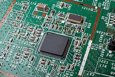
Generally, technological revolutions result in discarding traditional CEM-3 and FR-4 because of their poor thermal conductivity. In their stead, we have seen market demand for highly integrated circuit boards with sound dissipation systems (high heat resistance in an outdoor environment). Today’s post gives a quick overview of Ceramic Substrate PCBs.
Contents
What is the Ceramic Substrate?
A ceramic substrate is a unique process PCB with a thermal conductivity of 9-20W/m.k made at high temperatures under 250°C. Manufacturers prepare the substrate by directly binding copper foil to aluminum nitride (AIN) or alumina (Al2O3) surfaces.
Its electrical and thermal performance makes it better than most metal core PCBs in the PCB industry.
Advantages of Ceramic Substrate PCB
Ceramic substrate PCB has several advantages, making it ideal for multiple products like;
Material advantages
- Since the copper layer lacks an oxide layer formation, you can use it in a reducing atmosphere.
- Secondly, it has tough chemical erosion resistance and versatile/hermetic packages that prevent water absorption.
- Thirdly, it is highly reliable in aerospace, resistant to cosmic rays, and does not contain organic ingredients.
- Then, you can achieve high-density assembly with low thermal resistance.
- It also has a low high-frequency loss and good electrical insulation performance, making it able to withstand the harsh external environment.
- Besides using a high temperature during soldering, a ceramic substrate has good solderability.
- In addition, you can safely operate it in temperatures up to 350°C.
- It is a lower and stronger electrical resistance metal film (alumina ceramic PCB).
- Further, ceramic circuit boards are cost-efficient and ideal for heavy-duty applications.
- Finally, it has a more matching thermal expansion coefficient and higher thermal conductivity.
Technical advantages
The LAM and DPC technologies are gradually replacing traditional boards like DBC and LTCC technologies for many reasons.
- For instance, laser drilling technology provides great application value since it’s accurate, fast, and efficient.
- Then, there are good electrical properties and high bonding strength between the ceramic and metal circuit layers.
- There’s also a through-hole connection that gives customers a customized product solution.
What are the Types of Ceramic Substrates?
According to the material
Al2O3
Our first substrate is by far the most commonly utilized in the electronics industry. Reasons behind its popularity are its electrical, thermal, and mechanical properties making it chemically stable and of high strength compared to other oxide ceramics. Al2O3 is also rich in raw materials.
Applications: The ceramic product is ideal for manufacturing several different shapes.
AlN (Aluminum Nitride ceramic board)
AlN ceramic-based printed circuit board has two significant features worth knowing;
- Expansion coefficient matching Si.
- High thermal conductivity.
However, it has disadvantages like being pricier than Al2O3 and even a thin oxide surface layer affecting its thermal conductivity. Fortunately, you can control the process and materials while manufacturing AlN substrate to get a product with good consistency. Also, technological advancements might soon consider the pricing of Aluminum nitride boards.
Applications: Substrates for electronic materials (packages) and heat sinks to transfer heat from hot spots.
BeO
Compared to metal aluminum, BeO has higher thermal conductivity and is suitable for applications needing high thermal conductivity.
Also, remember that it is sometimes toxic and, therefore, not commonly developed.
Conclusion: As we have seen, alumina ceramics have properties and superior comprehensive performance that still make them dominant in various fields. For example, they are found in power modules, hybrid microelectronics, and power electronics.
They provide high mechanical strength, chemical stability, good dielectric properties, and thermal properties.
According to the manufacturing process
High-Temperature Ceramic PCB/High-Temperature Co-Fired Multilayer Ceramic (HTCC) circuit
This PCB type can withstand high temperatures (above 1300 Degrees Celsius). The unique manufacturing process involves creating new ceramics by combining lubricant, aluminum oxide, adhesive, plasticizer, and solvent.
Afterward, manufacturers coat the new ceramic and apply a circuit pattern tracing on tungsten, manganese, or molybdenum precious metals. They bake the circuit boards for about 48 hours at temperatures ranging from 1300 to 1700°C after lamination in a gaseous environment with hydrogen gas.
However, because of high co-firing temperatures, it lacks many metal conductor materials.
Low-Temperature Ceramic PCB/Low-Temperature Co-Fired Ceramic (LTCC) circuit
Manufacturers use crystal glass materials and adhesive substances (organic binder) to create low-temperature ceramic PCBs. They apply both materials to a metal sheet that has gold paste. Then, they cut and laminate the board before placing the PCB in a gaseous oven at 900°C.
Advantages
- It has less warpage and better shrink than HTCC.
- Additionally, it has higher mechanical intensity and thermal conductivity than other substrate types.
Applications: Heat-free products like LED lights.
Thick Film Ceramic PCB
In a thick film process, manufacturers coat gold and dielectric pastes on a ceramic base material. Then, they bake the material at 1000°C or lower operating temperature. They prefer a thick film ceramic due to its ability to prevent copper oxidation.
Thus, the manufacturers can use electronic components like resistors, electric capacitors, conductors, semiconductors, and interchangeable conductors on the ceramic board.
It is often a preferred choice when worried about oxidation. Also, the conductive layer of a thick-film ceramic PCB board shouldn’t be thicker than 13 microns.
- DBC (Direct Bonded Copper)
The technology utilizes an oxygen-containing eutectic solution of copper to place metal copper directly on the ceramic circuit board. Often, its basic principle involves introducing a required amount of O2 between ceramic and copper during or after a deposition process. The two materials form a Cu-O eutectic liquid in thermal ranges between 1065 and 1083°C.
- DPC (Direct Plate Copper)/ Copper-plated substrate
The ceramic material option often undergoes the process below;
Manufacturers begin by pre-processing and cleaning the ceramic substrate. Then, they use a professional film manufacturing technology coating method to sputter and bond a copper metal composite layer onto the substrate.
Next, the photoresistor with yellow light lithography undergoes re-exposure, development, and etching. Finally, the film removal process becomes complete, and now the manufacturers increase the circuit thickness by electroless/electroplating plating deposition.
Removing the photoresist completes the metallization circuit.
- LAM (Laser Activation Metallization)
The rapid laser technology ionizes meta and ceramics using a high-energy laser beam. Afterward, it lets the two components grow together, enhancing their firmness during the metallization process.
Application of Ceramic PCB
Due to its features like high thermal conductivity, low dielectric constant, etc., ceramic PCBs are in the applications listed below;
- Street, high bright light,
- Semiconductor process equipment,
- Telecom device,
- Sensor,
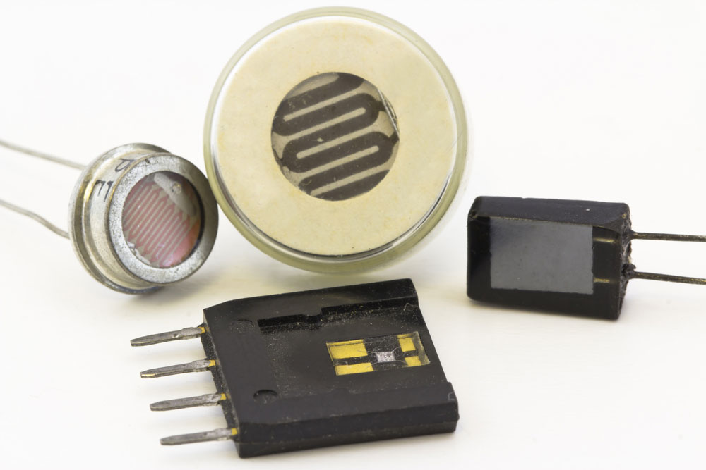
(different types of sensors)
- Solar cell,
- Automotive light system,
- LEDs,
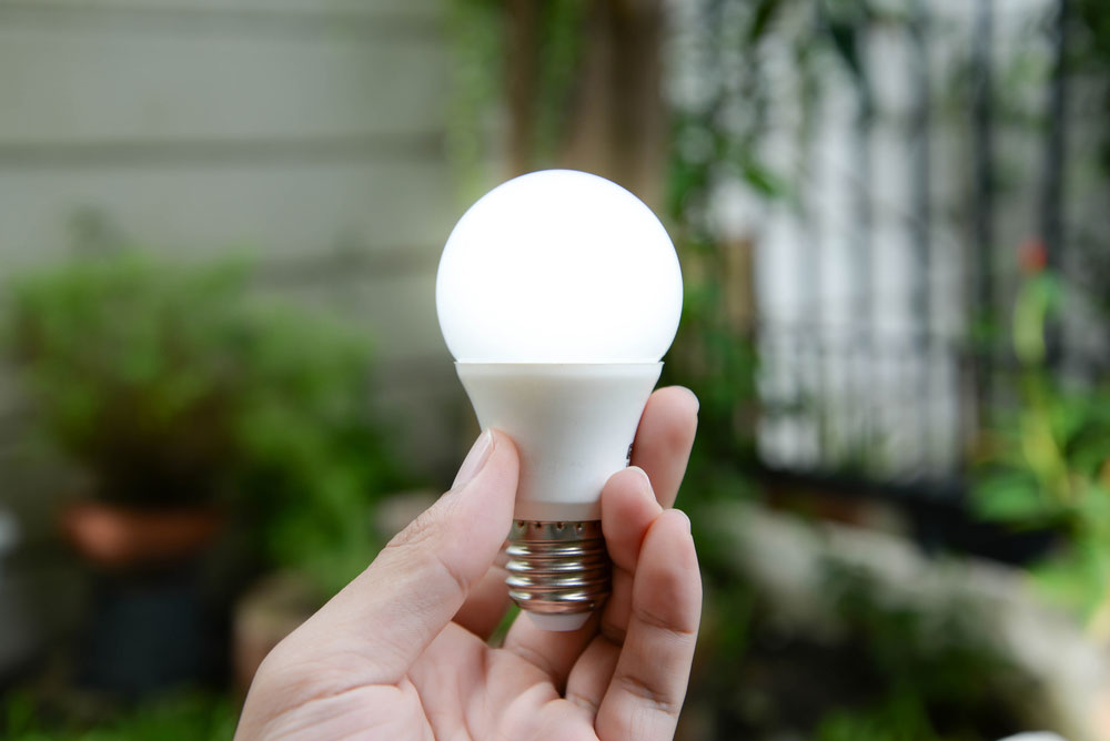
(LED bulb)
- Digital and Analog PCB,
- Transmission/Receiving module,
- Solar panel arrays,
- Solid-state relay (SSR),
- High-accuracy clock oscillator, OCXOs, TCXOs, VCXOs,
- High-power circuits,
- Chip-on-board module, and
- Memory module.

Ceramic PCB VS FR4
We’ll now compare the ceramic multilayer and FR4 board materials based on several criteria below.

Disadvantages of Ceramic PCBs
Despite their high uptake, ceramic PCBs still have downsides that would make a manufacturer recommend alternatives.
Intricate PCB design
- Ceramic PCBs are relatively expensive. The price of a ceramic substrate PCB can range from $50 to $200 per square foot. The price difference might be caused by design complexity, layering, and additional features during design and manufacturing.
- Ceramic PCBs also present a handling challenge. Ceramics are fragile, so the manufacturer must take precautions to minimize or prevent damage during handling. This might mean a rise in the cost of handling, especially in logistics.
- You may need special tools and processes. Manufacturers opt for ceramic PCBs for tight spaces, so the PCBs must be miniaturized. Picking highly precise tools to reduce any risk of damage makes assembly and handling more challenging.
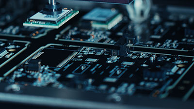
How To Manufacture Ceramic PCB?
Manufacturing ceramic PCBs involves a dozen processes.
- Circuit Layer Design: This stage uses CAD software to place functional traces, vias and PCB components. At this stage, the manufacturer is attentive to signal integrity and heat sensitivity.
- Preparing the ceramic substrate: This is where mixing is done. The manufacturer follows design and fabrication requirements to check the best mix for the required application. The final substrate is then cut and shaped. Finally, the manufacturer adds a surface finish.
- Preparing layers(if it’s multiple layers): Every layer to be used is prepared and set aside individually. They are stacked after each layer has been designed to specifications.
- Adding conductive material: Screen or inkjet printing applies conductive material to the ceramic. The conductive material could be silver or gold pasting.
- Creating Vias: Depending on the PCB size and density, specialized drills are used to drill vias. The vias enable the connection to different layers of the PCB. However, the connection is only complete after the vias are filled.
- Sintering: Due to the ceramic’s high heat tolerance, it is fired in a furnace at temperatures slightly below 1000 degrees Celsius to fuse the ceramic and conductive pasting in step 4.
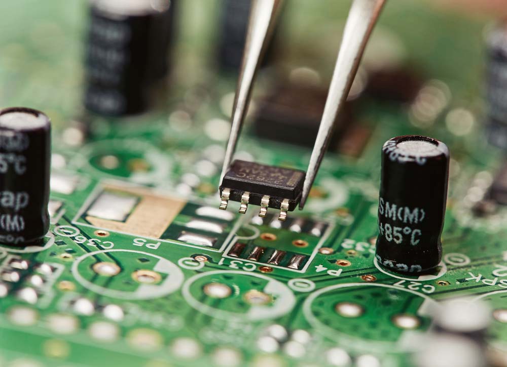
- Adding components: Once any additional layers are added, SMDs are soldered into the ceramic PCB.
- Quality assurance testing: At this point, the ceramic PCB is almost done. Therefore, it is tested to check for functionality. The board is put through various visual and conductivity tests.
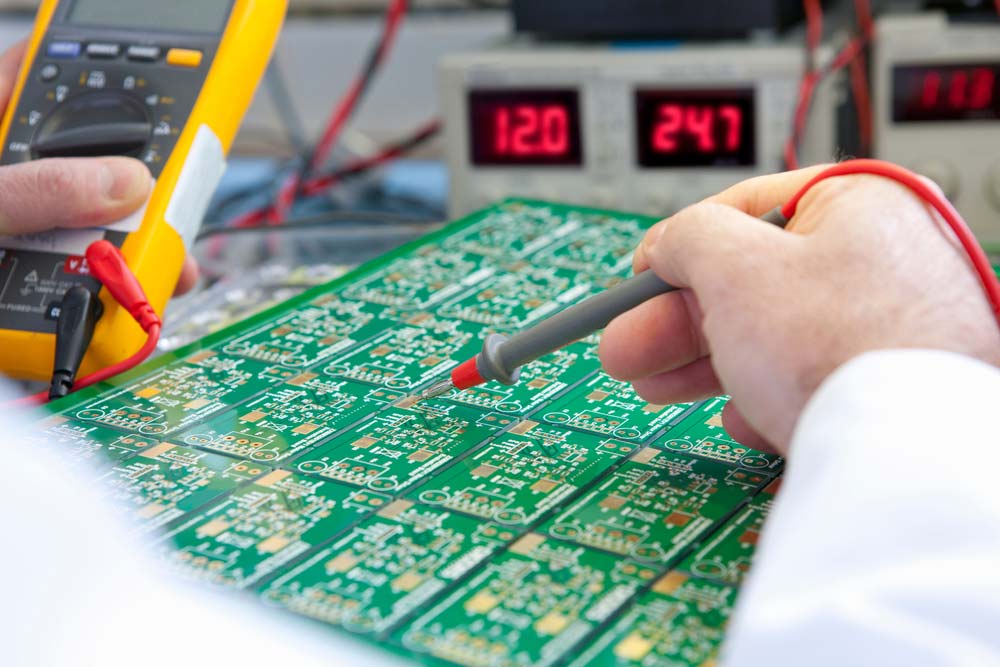
PCB inspection
- Finishing: Once the ceramic board passes the QA tests, it is coated and finished. Manufacturers add protective layers to prevent moisture, chemical and heat damage.
- Final tests: the finished ceramic PCB is assessed and checked against the design specifications. Once full functionality is certified, it can be packed and delivered.
When is It Ideal to Use Ceramic PCB?
Even with its superior qualities, manufacturers won’t always go for ceramic PCBs. However, some applications demand that you choose ceramic PCBs.
When The Equipment Is Vulnerable To Corrosion.
Ceramics are highly resistant to corrosion, so they’d be suitable for applications with high condensation and humidity. However, most high-heat dissipating equipment might have moisture as a residue, which would compromise its durability and function.
When You Want Shape Retention
Applications that dissipate excess heat might change the shape and form of PCBs. However, ceramic retains its structure when there are erratic heat changes.
When You Need To Keep The Weight Low
Since ceramic PCBs are lightweight, you can layer them without burdening the equipment with excess weight. It makes it ideal in industries such as aerospace and marine equipment.
When You Need High Thermal Conductivity
Ceramics have a standard thermal conductivity of 170-180 W/M/K. Such thermal conductivity means you can protect the inner layers of high-heat equipment from heat damage, improving their durability.
Conclusion
In conclusion, ceramic circuit boards are efficient in several industries, like the electronic industry depending on your manufacturing needs and designs. They also provide quality features like thermal efficiency, good electrical conductivity, and mechanical strength.
Kindly contact us if you wish to know more about ceramic substrate materials.