Contents
What is Via Plugging?

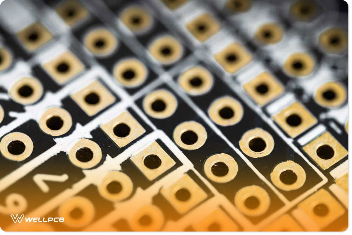
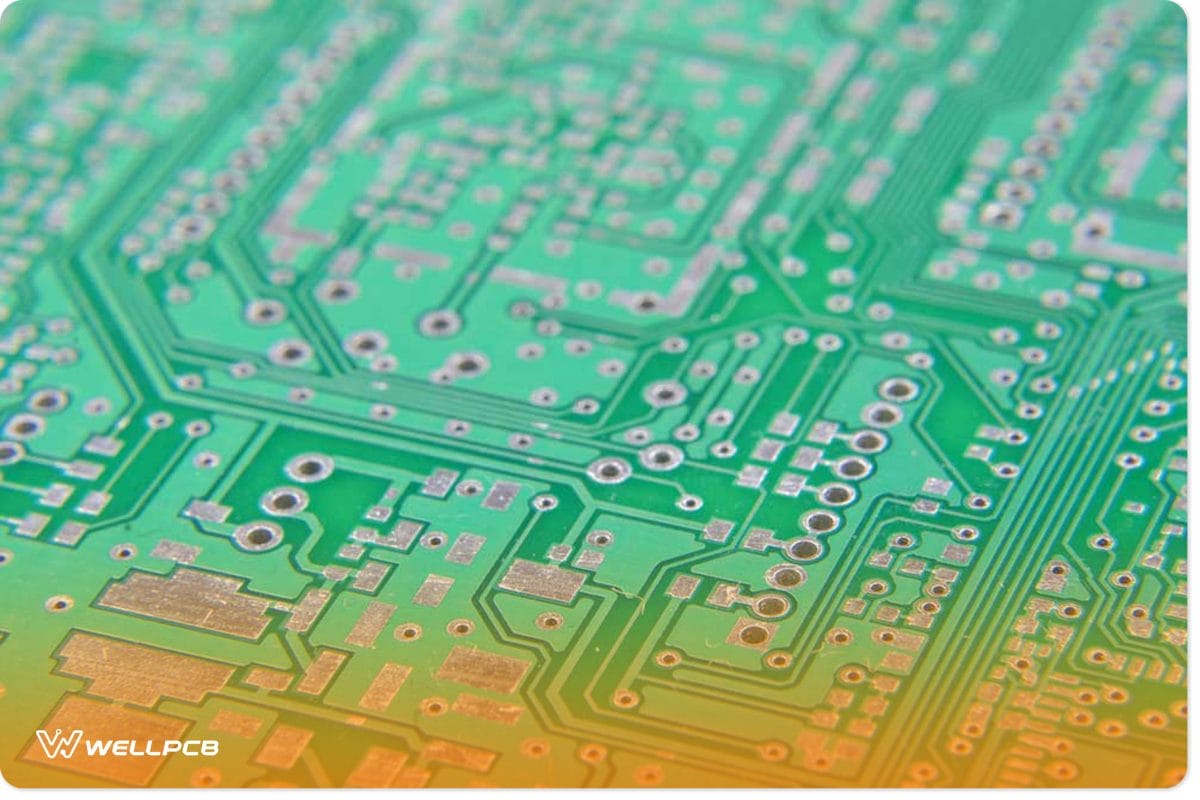
PCB
Via plugging is a technique manufacturers use to fill vias with resin or solder masks. It’s the exact opposite of via tenting, where manufacturers cover the holes, not plug them.
You can think of plugging as a protective measure. It prevents extra solder material from flowing into the plated hole during soldering or assembly.
In other words, unplugged vias create free openings for unwanted solder to flow and cause solder joints. Interestingly, manufacturers can use non-conductive and conductive materials to plug vias.
Further, using non-conductive materials to fill via holes won’t affect their functions. But, the drawback is they won’t be durable enough to handle higher current loads.
In contrast, vias plugged with conductive materials will easily support large current loads from one layer to another. But there’s a catch. Vias with conductive materials may have high CTE (coefficient of thermal expansion).
So, there’s a high chance that the conductive material will heat and expand faster than the surrounding laminate. Unfortunately, such situations can create fractures between the via wall and the concerned contact pad.
Plug Via Process
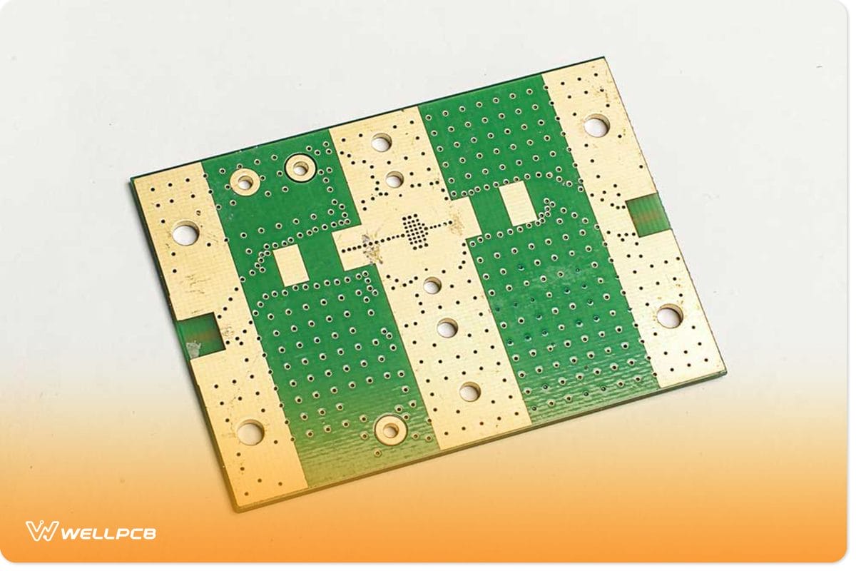
Multiple PCB vias
As mentioned earlier, we have two methods of via plugging–but this depends on the material used (conductive and non-conductive materials). Between these two, the non-conductive via plugging is more widespread. So, let’s take a closer look at these methods.
Conductive Via Plugging
This plug-via process is ideal for PCBs designed for applications involving the transfer of currents in large amounts–usually from one layer to another. Also, conductive via plugging provides excellent heat dissipation qualities.
Pros
- Conductive via plugging provides heat transfer or sink in areas where standard methods won’t reach–like a chip component’s base.
- It offers enhanced thermal conductivity, which increases current carrying capacity. The material’s conductivity may range between 3.5 to 15 W/mK.
Cons
- This process may cause instability for the copper plating and pad inside the via. This problem occurs due to the CTE value difference between the surrounding laminate and conductive material.
- More pricey than its non-conductive via plugging counterpart.
- Not many people demand conductive via plugging.
Epoxy Resin or Non-Conductive Via Plugging
This process is more popular than conductive methods. Here, manufacturers fill the via hole with non-conductive materials. The plugging material depends on a few factors, like design requirements, availability, CTE value, and plugging machine type.
However, the thermal conductivity of this process is usually 0.25 W/mK. But despite this low value, the plugged via won’t transmit weak signals or zero currency. Further, it’s hard to spot the difference between vias on a standard PCB and those plugged with non-conductive materials.
Pros
- Non-conductive via plugging is more stable and reliable. In addition, unlike conductive materials, these fillers have matching CTE with the surrounding laminate.
- It stops the intrusion of solder and other contaminants.
- Non-conductive via plugging is strong enough to provide structural support for active pads.
Cons
- It may not handle high currents due to low thermal conductivity values.
Tenting Vias, Plugged Vias, and Via in Pad
PCB with vias
You might get confused between tenting vias and plugged vias when making your PCB order, but this section is here to enlighten you on the differences.
Functionality
Tenting is widespread in PCB fabrications and only involves using solder masks to cover the via hole & the annular ring.
It’s particularly effective for preventing element exposure and reducing unwanted contact or shorting.
However, manufacturers don’t take specific steps to ensure all via holes remain closed, making it less functional.
Plugged vias, on the other hand, involve filling the via with ink. As a result, manufacturers follow specific measures to ensure all vias stay plugged and sealed with masks. Also, the aperture yellowing problem tenting doesn’t get solved via plugging fixes.
Via-in-pad is different from the plugged and tenting via. The process doesn’t receive any treatment during PCB fabrication and drills your vias directly into the BGA footprint pad.
Of all three, plugged vias offer the best functionality.
Design Requirements
Fabrication notes are necessary if your designs require tenting files. You can do this in a Gerber fab drawing or a readme.txt file.
The Gerber fab is more detailed and signifies intentions to remove some masks. Manufacturers may put your order on engineering hold if it doesn’t have this information.
Also, you should notify your manufacturers if you need plugged vias for your design. Like tenting, you can place it in a readme.txt file or specify it in your fabrication print.
Additionally, you’ll need details like size, quantity, and location of the vias you want plugged in.
It’s crucial to call out the via-in-pad requirements in your fab notes before sending them to your manufacturer.
Pros and Cons
One advantage of the tenting process is how easy it is to perform. It’s a one-step process that manufacturers can complete quickly.
However, tenting doesn’t guarantee total protection.
On the other hand, all plugged vias are 100% filled and tented. Moreover, plugged vias may require additional processes to complete and cost you extra.
Rounding Up
Printed circuit board
Plugged vias are a necessary process that ensures the total protection of your vias.
Despite its disadvantages, plugged vias are still widespread for easier assembly and soldering.
In addition, manufacturers can use two materials to fill up PCB vias.
The conductive material would be perfect for high-speed PCBs, while non-conductive ones are ideal for low-current applications.
Lastly, ensure you send your required Gerber files to prevent any issues with the manufacturer.
Do you have any questions? Feel free to contact us, and we’ll be happy to help.