The pitch size is reducing significantly as the electronic devices are getting smaller and smaller in size. The demand is to place the electronic components on a printed circuit board (PCB) similar to how grains will pack in corn ears. Therefore, the increase in pin count on PCB has contributed to the invention of Ball Grid Array (BGA) soldering. You would find it amongst the most valuable product packages.
However, you would be wondering about the best way to solder BGA or how the solder defects can be recognized and treated. The BGA itself is shrinking in size, and the collapsed solder balls are unrecognizable by the naked eye. This article addresses all these points and much more. Let’s get started.

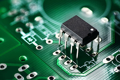
(It illustrates a close-up of BGA technology on a PCB)
Contents
- 1 1. Ball Grid Array Soldering– What is BGA (ball grid array soldering)
- 2 2. Ball Grid Array Soldering– Features of BGA
- 3 3. Ball Grid Array Soldering– Common types of BGA
- 4 4. Ball Grid Array Soldering– BGA welding process
- 4.1 4.1 The basis of BGA welding
- 4.2 4.1.1 Welding temperature
- 4.3 4.1.2 Welding kit and welding machine
- 4.4 4.1.3 Thoroughly clean your PCB
- 4.5 4.1.4 Ball Grid Array Soldering– BGA cleaning method
- 4.6 4.2 Ball Grid Array Soldering– BGA solder joint inspection
- 4.7 4.3 Ball Grid Array Soldering– Basic welding process of BGA
- 4.8 4.4 Ball Grid Array Soldering– Reflow soldering of BGA
- 5 5. Ball Grid Array Soldering– Solder defects in BGA
- 6 6. Ball Grid Array Soldering– BGA rework the problem
- 7 Summary:
1. Ball Grid Array Soldering– What is BGA (ball grid array soldering)
BGA is a surface mount device (SMD) that makes electrical connections via an arrangement of solder balls. It does not have any leads, and the package contains an assembly of metal spheres built of solder and referred to as solder balls. You would find these solder balls attached at the backside of the BGA package to a laminated substrate.
The BGA chip is attached to the substrate via flip-chip technology or wire bonding. On the inside, the BGA has an interior conductive traces that connect between substrate bonds and the chip. Further, it also makes a connection between the BGA bonds and the substrate. You can differentiate between a BGA package and other packages by looking at the pins, as BGA has solder metal balls instead of the nails. These solder balls give it a high lead count that is even more than 208 leads.
When compared with other packages, BGA is in demand in industries employing high I/O devices. The next section discusses in detail why you would prefer the BGA package over other packages.
")
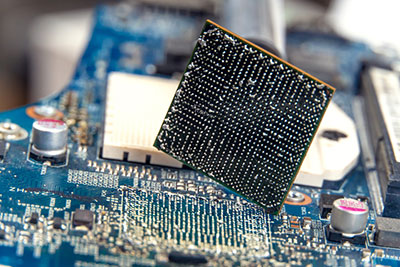
(It depicts a close view of BGA IC)
2. Ball Grid Array Soldering– Features of BGA
Advantage:
Lower trace density improves PCB design: In packages such as quad flat packs, the trace density is considerably high as the pins lie nearby. However, BGA solves or considerably mitigates this issue by spreading the contacts over the package’s whole surface.
Rugged BGA package: You would know that quad flat packs have sensitive pins as you can quickly destroy them even if you are very careful. Further, as the hooks have very pin pitch, it is almost impossible to repair the bent pins. However, there is no such problem in BGA. In BGA, pads and solder balls provide the electrical connections, which are not easy to damage.
Lower thermal resistance: Again, the quad flat pack has high thermal resistance, but BGA provides a much lower thermal resistance in the silicon chip. If your BGA integrated circuit generates heat, it will quickly and efficiently travel from the package to the PCB surface.
quad flat pack (QFP)
Improved high-speed performance: In BGA, the conductors are at the bottom of the chip carrier. It means that the length of the leads inside the chip is smaller. It, in turn, leads to a lower level of unwanted lead inductance. The unwanted lead inductance is responsible for the distortion of the unwanted signals in circuits operating at high frequency and speed. Therefore, with BGA packages, you can get high performance compared with their equals, the quad flat pack (QFP).
Reduced Package Thickness: With BGAs, you get the reduced thickness and can effortlessly manufacture PCBs for slim electronic products such as smartphones.
Practical usage of PCB space: You can productively use PCB space with BGA chips. You can make electrical connections beneath the surface of this SMD chip. You no longer need to limit the links to only the periphery of the SMD packages.
Can develop small IC packages: The standard SMD devices such as pin grid arrays and dual-in-line had overcrowded pins, with a tiny area between them. It is a disadvantage as you can accidentally solder together two or more pins. Nonetheless, with BGAs, you would not encounter any such issue and easily manufacture small IC packages.

(It shows BGA footprint on PCB)
Disadvantages:
Well, you know everything is not perfect, so BGA does come with few drawbacks. First of all, if you are naïve and not an expert in dealing with BGAs, you will encounter difficulty designing and making their circuits. Secondly, it is sometimes hard to inspect the faults in a BGA package. Thirdly, BGAs are non-ductile. Finally, it has a high cost, which can or cannot be a disadvantage depending upon your budget.
3. Ball Grid Array Soldering– Common types of BGA
Plastic BGA
Plastic BGAs (PBGA) are the most in-demand BGAs thanks to their low cost. They have ball pitch in size ranging from 1 mm to 1.27 mm. You would find these BGAs wrapped in a glass-mixture laminated substrate, plastic-coated body, and engraved copper traces. With them, you would get preformed solder balls and enhanced temperature stability.
If you wonder about their application, you can use them for devices requiring mid to high-level performance. Such devices need low inductance, high-reliability levels, and ease of surface mounting. Plastic bags also have additional copper layers, which can assist in increasing the power dissipation level.
Ceramic BGA
Ceramic BGA (CBGA) is among the earliest types of BGAs. It comes in a rectangular or square shape ceramic package that utilizes solder balls rather than leads for producing external electrical connections. CBGA lies in a grid present at the backside of the body of the box. You can use them in laptops, telecommunications systems, and device-under-test device applications.
Flex tape BGA
In this type of BGA, the flex tape, the chip, and the solder balls lie at the backside of a metal heat spreader. This heat spreader serves as the carrier and stiffener of the flex tape BGA package. The chip is connected to the tape traces via wire bonding and then put in a sheath. If you want to compare them with QPFA and PBGAs, their reliability, electrical and thermal performance is indeed better. You can use them for solutions demanding high thermal performance without heat sinks.
High profile high thermal conductivity metal top BGA
Like flex tap BGAs, you can also achieve higher electrical and thermal performance with high profile high thermal conductivity metal top BGAs. Their design is somewhat similar to flex tape BGAs. The chip is attached to a slug or heat spreader’s backside, reaching the package’s top. Therefore, because of the copper heat spreader reaching the package top, you get significantly lower thermal resistance, and the package surface is freely available for airflow.
If you also need to use a heat sink or other passive or active thermal management devices, you can couple the heat slug with them. Further, if you design extra ground and power planes, you will get enhanced electrical performance. With this type of BGA package, the disadvantage of BGA packages being difficult to inspect is no longer valid. Its top surface is highly reflective, so vision systems give superior performance when utilizing a diffuse lighting source rather than a polarized source.
Chip scale package
This BGA package gets its name because you can design it according to your chip’s size requirements. Any BGA package is a chip scale package (CSP) if it fulfills your chip specifications and is a surface mount device. You can use them in smartphones, smart devices, laptops, and other advanced compact electronic devices.

4. Ball Grid Array Soldering– BGA welding process
4.1 The basis of BGA welding
4.1.1 Welding temperature
You must select the right welding temperature and the solder alloy structure for welding or soldering BGA devices. As a quick tip, you can ensure that the BGA chip’s solder is not entirely melting. You might leave it in half-liquid form, allowing each solder ball to stay separate from other solder balls.

(It demonstrates a technician putting solder balls on ball grid array)
4.1.2 Welding kit and welding machine
Fortunately, a broad range of welding machines and welding kits are available for the BGA in the electronics market. In this technological era, you can also order them online. You may want to consider the following main features while purchasing the welding machines:
They should allow you to mount manually, solder, desolder, and remove your BGA chip.
May have reworking capability for both SMDs and BGA.
It can have inbuilt hot air heaters and infrared heating plates.
It would have a touchscreen operating system for ease of use.
You can use it for precisely controlling the solder temperature.
It may have emergency protection.
4.1.3 Thoroughly clean your PCB
Okay, so now that you have a welding machine or kit and have chosen the perfect welding temperature to start, it is still not enough. Before beginning the soldering of BGA, you still need to clean PCB and BGA thoroughly. For BGA, the requirement is to make it’s surface smooth. Let’s see in the next section how you can clean them step by step.
4.1.4 Ball Grid Array Soldering– BGA cleaning method
First of all, you need to position the BGA on a conductive pad and add a small quantity of solder paste onto its surface.
Next, use soldering iron and wire to separate the ball from BGA. Let the soldering iron liquify the tin ball and heat the permeable wire before you move the washing line over the surface of BGA. Furthermore, you should make sure that the soldering iron does not cause too much pressure on the surface, as it can result in surface cracking.
Use industrial alcohol for cleaning the BGA surface and friction motion to eliminate the BGA surface solder aid. Often start with the edges and do not neglect the corners. Keep going and wiping. Use a clean solvent for every BGA.
Then, you may also check the BGA surface for any unremoved tin balls and damaged pads using a microscope.
Disinfect the BGA surface with the brush and the deionized spray. Disinfect the BGA surface with the meeting and the deionized spray.
Clean the BGA surface with a brush and deionized spray. It will assist in eliminating the BGA surface remaining solder paste. Leave BGA in the air to dry up. Test the BGA surface twice.
For eliminating moisture, bake the BGA and PCB for 10 to 20 hours at 80℃ to 90℃ temperature in a constant temperature oven. You may regulate the baking time and temperature according to the level of moisture.
Furthermore, wear antistatic gloves or static rings in all subsequent operations to prevent unnecessary chip disruption due to static electricity.

(It is another close-up of BGA)
4.2 Ball Grid Array Soldering– BGA solder joint inspection
Importance of solder joint inspection
PCB manufacturers do not utilize the optical methods to examine BGAs because the solder joints under the BGA components are not visually visible. The electric appraisal is not very accurate because it shows only thBGA’s e electric conductivity only at that precise moment. It does not estimate the life of the soldier. The solder joint can deteriorate with time.
X-ray inspection method
X-rays monitor the soldering joints of the BGA. The X-ray analysis allows you to see at the soldering joints below the parts. Consequently, the industries extensively utilize the Automatic X-ray Inspection (AXI) technology for BGA inspection.
4.3 Ball Grid Array Soldering– Basic welding process of BGA
One of the main issues with BGA was if it could deliver a successful welding or soldering operation. Also, since the BGA chip has pads instead of pins at its backside, it is essential to follow a proper welding method.
Fortunately, BGA welding techniques have demonstrated that they are more effective than standard quad flat packs. You only need to ensure that you correctly set up the process. Henceforth, this means that the PCB assembly prototypes and the PCB assembly production on a broad scale.
Before beginning the BGA welding process, you must carefully select the solder and ball’s size and the collapsed height. You will heat the solder balls, and when they melt, the surface tension will allow them to fit the BGA with PCB correctly. After that, the solder will cool and set down, preparing the BGA PCB.
However, this heating of solder balls is not as simple as it sounds. You will need to use reflow soldering methods for this purpose. It is crucial as you must ensure that the solder under the BGA chip melts. To this end, the entire assembly needs to exceed the melting point temperature. Ultimately, only reflow processes can do it.
4.4 Ball Grid Array Soldering– Reflow soldering of BGA
Flux selection: water-soluble and no-clean
Okay, so now that you know why we need to use a reflow soldering procedure, we will move onto what type of flux you should use. There are essentially two forms of change: water-soluble and no-clean. You may use no-clean flux if you cannot wash the circuit board with deionized water at the final reflow soldering and PCB assembly stages. You may not want to pass the circuit board if it contains LCDs, crystals, or more water-sensitive parts.
On the other hand, you can use water-soluble flux when you intend to wash your PCB with deionized water. It is worth noting that the flux type defines activity level among the change activity and the solder paste, regardless of what kind of flux you use.
Solder selection
Finally, after selecting the flux, it is also essential to choose the right solder. Insufficient reflow, inadequate change, and low stencil printing can all lead to open solder ball failures.
5. Ball Grid Array Soldering– Solder defects in BGA
We just mentioned the word open solder ball failure. It is a type of solder defect and is also known as an available solder joint or non-collapsed ball. Its cause is inadequate heat during reflow. BGA intermittent connection (BIC) is another type of solder defect. It impacts all pitch sizes and is extremely dangerous as it is frequently irregular. It can cause loss of OEMs thousands of dollars hidden in wasted manufacturing time and delays in a product release.
Nevertheless, as its name suggests, BICs collapse only occasionally. Since they are hard to find, BICs will create a chain reaction by sending the elusive, difficult-to-track design dilemma to several OEM engineering groups and finally to the management board.
Besides non-collapsed balls and BICs, you must also take shorts, opens, and cracked BGA balls. As with non-collapsed balls and BICs, a weak thermal profile for the reflow causes these defects.
A thermal profile defines the temperature range under which you will warm a PCB during reflow soldering and also the time spent by the board at any temperature. If you properly plug in all temperature zones of a thermal profile, the outcome is a complete reflow. You can then verify it by a BGA X-ray inspection.
6. Ball Grid Array Soldering– BGA rework the problem
6.1 Ball Grid Array Soldering– Manual BGA Desoldering
You need to update if you didn’t correctly solder for the first time. If you do not use the rework to remove the component, you need to heat the PCB around the element so that the solder is again melted (desoldering), and the welding improves. If you need to disconnect the component and solder, then rework and hand soldering the BGA Packages are the most complicated parts. Let’s go through it in the next sub-section.
6.2 Ball Grid Array Soldering– Manual BGA welding
1: Detach the BGA, and carefully wipe away any remaining PCB pad solder.
2: Next, check that there is no moisture on BGA as it is moisture-sensitive.
3: Select a small BGA template for printing the solder paste. You must use the ball distance and diameter to determine the opening size and thickness of the template. In the end, you shall also inspect the quality of printing.
4: Use a soldering iron to clean and level the residual solder. You may further use a flat soldering tip and a disassembly belt. Be careful not to damage the solder mask and pad.
5: Repeat steps 2 and 3.
6: Now, it’s time to mount the BGA. It would help if you placed the surface PCB assembly plate (after printing) onto the workbench. After that, you must switch on the vacuum pump after choosing a proper suction nozzle. The nozzle will swallow the BGA chip, bring it down when the PCB pad and BGA overlap. Finally, integrate the BGA chip with the PCB, and shut the vacuum pump.
7: Select an appropriate reflow soldering temperature conferring to the PCB thickness, your device size, etc. In general, the BGA temperature is 15 degrees more than traditional SMDs.
8: You are all set now. The final step is to inspect the BGA welding.
Summary:
In this article, we have introduced BGA technology, its different types, advantages, and disadvantages. Further, we have explained what welding kits and machines you may buy for soldering them. And, if you didn’t solder well, how can you do the BGA rework.
We have also compared the BGA with traditional surface mount devices. Finally, we also presented solder defects so that you may avoid them. If you still want more information related to BGA technology, you can contact us and discuss it together.