When designing or building a circuit board, sometimes it may feel like it takes forever for you to accomplish the final design. Sometimes it’s because of meddling with your copper and solder, trying to make sure that you finally print printed circuit board in the end, or maybe even design problems like through-hole technology or layout design with pads, vias, and any signal integrity problems.
By following the right procedure step by step, you will avoid future mishaps, and in case you find yourself on the wrong side, troubleshooting will not be a pain. So without further ado, let’s jump right in.
Contents
- 1 Verify Board Layout and Layer Stack
- 2 Give Space Between Components
- 3 Exchange Wiring Directions Between Layers
- 4 Select The Width Of Lines Depending On The Current
- 5 Determining Routing And Vias
- 6 Building a Circuit Board– Avoid 90º Angles With Traces.
- 7 Building a Circuit Board– Consider Spots of Heat
- 8 Building a Circuit Board– Always Use the Same Symbol for the Same Device
- 9 Building a Circuit Board– Tips for Mixed-signal Circuits
- 10 Building a Circuit Board– Make Sure Every Part Has a Unique Designator
- 11 Building a Circuit Board– Know the Specifications of the Manufacturer
- 12 Summary
Verify Board Layout and Layer Stack
In case you have been doing this for a long time, you know how important it is to know your design software. It ensures that you get your Printed boards designed the right way. Placing traces for routing and copper placement or running the layer needed for solder can sometimes be challenging without a precise and dependable integration from schematic capture to the layout.
You can verify your circuit board layout by using a design rule check (DRC). When you move your schematic data to the PCB Doc. the component footprints will be on display in addition to the board outline specified. Before you place the components, you have to define the PCB layout. the shape, stack up, and layer using the stack up manager.
Give Space Between Components
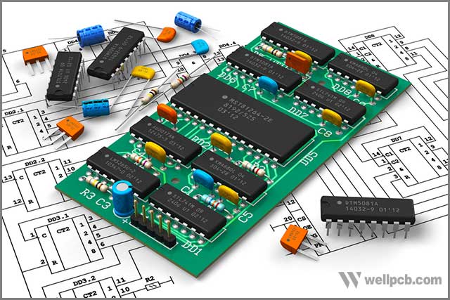
Although it is sometimes compelling to stack all the ingredients tightly packed to each other. you might find out later that there is not enough space for routing your circuit. Therefore, it is essential to leave some room between the components so that wires have room to spread.
Usually, the more pins the component contains, the more space will be needed. Spacing your elements also facilitates ease in soldering. Generally, how well you place your components will define how easy it will be to manufacture your board.
Exchange Wiring Directions Between Layers
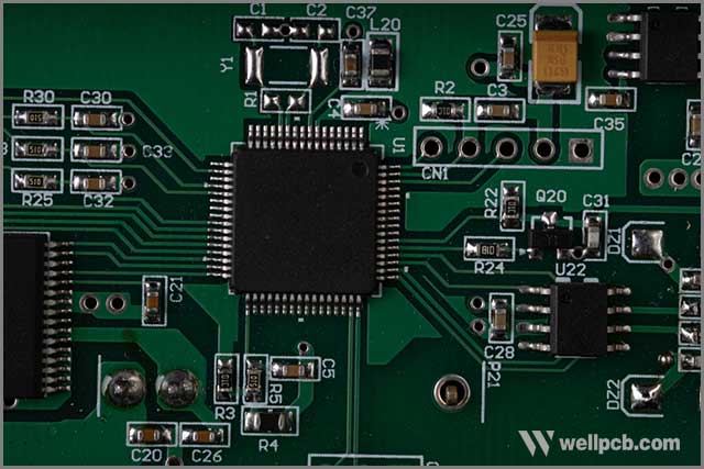
When considering the PCB layout, it is significant to ensure that the wiring direction is different in the successive layers. For instance, if the horizontal wiring is in use on a particular segment. then vertical installation should be used in the succeeding layer. This pattern should be repeated in all the layers if you are dealing with a multilayer PCB.
On the other hand, drawing horizontal traces on one side and vertical marks simplifies the wiring of lines that have crossed over other lines. So for a PCB with multiple layers, it is advised to alternate between directions.

Select The Width Of Lines Depending On The Current
A circuit board performs best only if it allows current flow flawlessly. The undisrupted flow of current is vital in the proper operation of the device. Therefore selecting a line width that does not hinder the flow of current is a smart way of maximizing the productivity of the layout.
Knowing the width of lines will enable you to plug your estimated current and thickness and therefore get a trace width value in return for external and internal layers. But in the case where you have the chance to use larger widths that your calculator suggests, you should not hesitate. As long as you meet your manufacturer’s requirements. the larger your traces are, the more likely your board will withstand broken connections.
Determining Routing And Vias
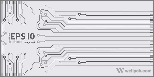
Routing adds wires necessary in the connection of laced components correctly. It would help if you tried to use the excellent routing guidelines and wisely use your desired software design tools to make the process smooth, such as color-coding via routing and highlighting nets.
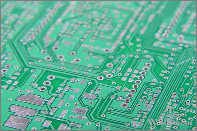
Via is an essential component when it comes to multilayered PCBs. They are used to interconnect different layers on and inside the multilayered PCBs. Vias are used to electrically ad thermally link traces, polygons, and pads to different PCB segments.
Usually, you place sacrificial vias in the PCB on a segment of the production board. This is so that you can slice the vias and inspect the cross-sections to determine the electroplating process’s efficiency.
Building a Circuit Board– Avoid 90º Angles With Traces.
It is a little hard to keep the trace width persistent with sharp right-angle turns. It should be the case, especially with narrow trails, where just a small difference makes a significant portion of the evidence. It’s, therefore, better to do two 45º bends. Also, you stand a chance of getting a lot of 90º angles marks back that are not entirely etched, leading to shorts.

Building a Circuit Board– Consider Spots of Heat
Heat can reduce circuits’ performance and sometimes even damage them when the heat dispelling is not done correctly. A parameter known as thermal resistance shows how much temperature is added per watt of power when you meet certain conditions. Apart from the components, the strength of electrical networks, vias, and copper traces all in a way contribute to heat production.
Designers are supposed to try producing PCBs that work and stay under safe temperature limits for designers to evade failures or circuit breakdowns. Some circuits work properly without added cooling, but there are certain situations where increasing heat sinks and cooling fans or both are unavoidable.

Building a Circuit Board– Always Use the Same Symbol for the Same Device
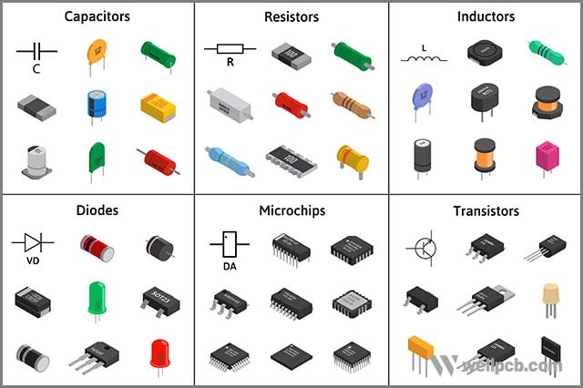
To be consistent with your schematic, you should always use the same symbol to represent the same device. For instance, putting an IEEE resistor on your schema and a European resistor will confuse you.
Before you design your schematic, you should take time to evaluate all of the identifiable electrical symbols and make sure you use the same symbols always in all your projects.
Building a Circuit Board– Tips for Mixed-signal Circuits
Keep digital and analog grounds separate
As for power circuits, PCB board, you need to keep the digital and analog grounds separate. This is necessary because voltage and current spikes emitted from the digital PCB board circuits can sometimes create interference in the circuits located in the analog. This can affect their performance. If you tie them together in the PCB, then you should bind them at the end of the supply path, preferably close to the PCB ground connection.
Protect analog grounds from noise
If there is any interference present in the analog ground, it’ll have similar effects as it would be in the signal lines. If you want a considerable ground plane to decrease its resistance, that causes it to be more vulnerable to capacitive coupling to lines routed either beneath or above it. With that said, the analog ground is supposed to have analog lines crossing it and also digital. Doing that decreases the capacitive coupling between analog and digital circuits.

Building a Circuit Board– Make Sure Every Part Has a Unique Designator
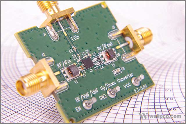
To improve the reliability and readability of your schematic, all the symbols in your circuit need to have their distinct designator to make every part identifiable. Every resistor is supposed to follow a consistent naming arrangement of R1, R2, R3, etc.
If you intend to use components with specific performance requirements, you should add a label to the symbol. An example is that you may have to increase labeling for parts consisting of specific trace width requirements, impedances, or special shielding.
Building a Circuit Board– Know the Specifications of the Manufacturer
Every manufacturer has its specifications, like the minimum trace width, the number of layers, etc. Before you start your design, you need to reflect on what you require and look for a manufacturer that meets your requirements. You should include the grade of materials of the printed circuit board in your needs ranging from, FR-1 to FR-5. FR-1 is also known as a paper-phenolic mixture, and FR- is glass cloth and epoxy.
With this info, you can set your trace width and want the spacing to be instead of re-routing the whole board layout.
You should keep in mind that the type of material you pick will affect the circuits board’s flame resistance, durability, strength, and moisture absorption.
Summary
11 Top tips to make sure that your circuit board production goes according to plan. WellPCB is a well-known reliable company that understands that customers are a priority. We have two modern PCB factories and one PCB assembly factory.
You can place any orders concerning Printed ordering, fast delivery, and low cost all our esteemed customers worldwide.


