Contents
What is a Ceramic Chip Antenna?
When comparing a chip antenna Vs. a PCB antenna, you should acknowledge Ceramic Chip antennas for their lesser spatial needs. Besides, you can easily include them in circuit boards to generate high-frequency electromagnetic frequencies. Nevertheless, they have limited RF ranges, making them ideal for small gadgets like Wi-Fi routers and smartphones. Generally speaking, Chip antennas produce and receive radio frequencies just like other antennas. It is only that they are smaller in size compared to PCB antennas. However, it is their small sizes that will allow you to mount them inside electronic products effectively. Besides, they are cheaper alternatives when you do not want to sacrifice product quality.
What is a PCB Trace Antenna?
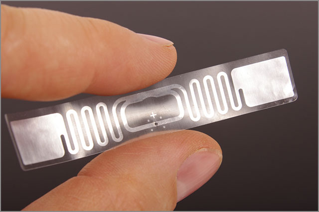
A PCB trace antenna consists of a trace drawn directly onto a circuit board. It is essential to realize that the antennae type and the space requirements determine the trace type. The PCB traces you can use include inverted F-shaped traces and straight, curved, meandered, and circular traces.
Generally, a PCB trace antenna acts as a wireless communication method. Furthermore, during PCB manufacturing, you should laminate your trace onto the board surface. But sometimes, PCB traces cover many layers, especially in multi-layered PCBs.
Ceramic Chip Antenna Vs. PCB Antenna: Pros and Cons
Ceramic Chip Antenna
Pros
In the Chip antenna Vs. PCB antenna debate, it is undeniable that the use of a Ceramic Chip antenna presents numerous benefits. Specifically, it removes the requirement for costly prototype production and simulation software. The antenna’s network-tuning capacity and the absence of physical properties guarantee the above benefits. Ceramic Chip antennas provide more benefits such as:
- They come as separate parts.
- You can easily get small sizes and numerous configurations for different designs.
- The proximity to other parts does not create adverse effects like in PCB Trace antennas.
- Environmental and human factors cause negligible impacts on Chip antennas compared to Trace antennas.
- They offer flexible tuning and testing alternatives.
- You can easily introduce design modifications.
Cons
Like anything else in this world, Ceramic antennas also have their dark side. Below are the cons of Ceramic PCBs:
- The initial antenna and logistics costs might be more expensive than that of a PCB Trace antenna.
- You require some RF knowledge for optimum implementation.
- It has a lower performance than a trace antenna.
PCB Trace Antenna
Pros
The proponents of the Chip antenna Vs. PCB antenna debate argues that a trace antenna is difficult to apply, create, and tune. This is particularly true in a consistent and small operation. Additionally, like a wire antenna, the ultimate bandwidth frequencies determine the size of a trace antenna. Below are the key benefits of a PCB trace antenna.
- Production costs are low since you integrate the trace into your board manufacturing process.
- A trace antenna can accommodate a wide bandwidth when maximally tuned.
- PCB trace structure is simple, and since you place the antenna on the surface, the structure profile is relatively thin.
- It provides better strength capacities and network reliability.
- You can easily insert it into your PCB during production.
Cons
These are the cons of a Trace antenna:
- It is hard to create, mainly at minimal frequencies.
- A trace antenna is highly prone to PCB layout modifications, calling for tuning after every alteration or reproduction.
- It demands ample space, more so at minimal frequencies.
- The need for a bigger board space raises the design expenses.
- They are susceptible to human and environmental factors.
Embedded Antenna Design Tips
Antennas are essential components of the wireless system. However, most designers often regard them as an afterthought. Planning for your antenna design at the beginning of your manufacturing process will capitalize on the product performance. Besides, it will also eliminate delays and reproductions in the later phases. Below are some crucial tips to assist you with the preparation of an embedded antenna design.
Materials
Whether you carve the antenna structure onto a board, plastic, or stamped metal, ensure these materials have steady dialectic properties. Low-cost dielectric FR4 board materials differ significantly from one supplier to the other. This is why you should specify your board materials from the beginning.
Physics Suggestions
To ensure your electronic device has a high range of performance, you need an effective antenna system. Additionally, you should allow adequate antenna system space. Therefore, please participate in the initial stages of your gadget production cycle. This will enable you to discuss and agree on the design choices. You will also have an opportunity to get rid of any potential compromises.
Product Location
When you place an antenna at the extreme ends of your product, it becomes sensitive to the immediate environmental conditions. Therefore, you should consider how you plan to use your product and where you intend to locate it. For instance, you should ensure that your antenna is not covered by the end user’s hands when held naturally for a hand-held gadget. For wall-mounted devices, ask yourself whether the consumers will fix them on metallic parts. This is because metallic surfaces significantly affect product performance.
Casings and Coatings
Do not cover your antenna in a metallic casing or use a metallic coating to have a high antenna performance. Besides, contact your mechanical and ID colleagues in your company to ensure the region surrounding your antenna is free of any potential upsetting materials.
Internal Structures
The location of inner metallic assemblies in relation to the antenna also influences the product performance. For instance, in wearable gadgets, the battery is the primary component of the general assembly. Therefore, you should define its location and function in your antenna design.
Antenna Weight
When you talk about an embedded antenna, you are referring to a physical component. For instance, the PCB carved part or the metalized case plastic section. But in most cases, this forms a single antenna system portion. The main system ground consists of the remaining half. Since this is usually the primary board ground, you must ensure enough weight to enable the antenna to vibrate appropriately.
Circuit Sensitivities EMI/RFI
Wireless systems comprise transmitters and receivers. The transmitter can interfere with the adjacent circuit. This makes the receiver vulnerable to interference from the local circuits. Therefore, you should position your antenna relative to sensitive circuitry to achieve high wireless product performance.
Antenna Frequency Detuning Challenges During Testing
Since the board layout significantly impacts the antenna performance, you need to tune it to achieve maximum system performance. It is essential to realize that appropriate electrical resistance matching produces all-out frequency transmission in the appropriate band.
With trace antennas, since the antenna design is inclined to the general board design, it is hard for you to carry out tuning and establish maximum performance. Besides, minimal dielectric board permittivity renders the antenna too vulnerable to design alterations and tolerance variants. In such cases, you need to re-spin your PCB to attain maximum antenna performance.
With Ceramic antennas, you can vary matching aspects to cater to the in-built detuning. Most engineers prefer the Π-type method as it provides the best flexibility regarding the working bandwidth tuning.
When designing your preferred matching network, you can use a Vector Network Analyser (VNA) to review your PCB test circuit. In addition, the VNA will help you to establish the antenna input resistance. You can find the S-parameter, the VSWR band, to get your on-PCB Ceramic antenna efficiency.
WellPCB provides Ceramic antenna optimization services. Our RF personnel will adjust the matching network to your preferred resistance using cutting-edge technology for maximum performance. It is important to note that matching enhances the antenna efficiency for the select bandwidth in the product working environment. Our personnel also evaluate design layouts for proper PCB space usage.
Final Thoughts on Chip Antenna Vs. PCB Antenna Comparison
Regarding the Chip antenna Vs. PCB antenna comparison, a Chip antenna experiences less detuning from human and environmental factors than a PCB antenna. Two antennas offer better antenna-to-antenna remoteness in multi-radio devices and outdo PCB antennas when choosing the optimal antenna type and implementing it accordingly.
You should test your antenna performance in the final, fully practical product using OTA measurements. With PCB antennas, assessment failures are costly and challenging to resolve and call for numerous board iterations. Remember, the Chip antenna is a separate part; therefore, you can easily and quickly improve it. You can twist the tuning and test the system performance by modifying the antenna part only. We hope that the Chip antenna Vs PCB antenna comparison guide will help you choose the right antenna for your embedded designs.


