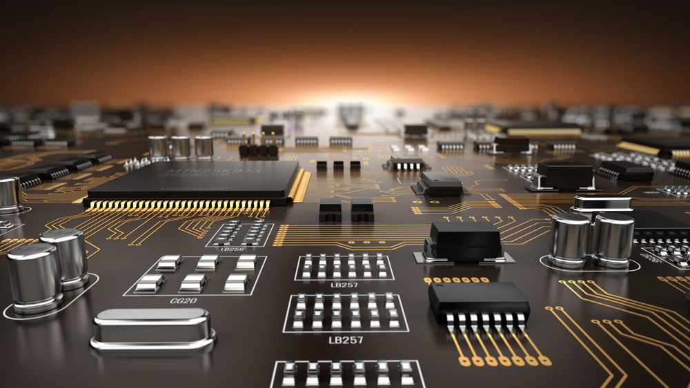
Custom PCB
- A custom PCB is a device that has its components soldered securely to its board.
- Hence, custom PCBs don’t face pull free or snagging issues because they have no wires.
- Plus, the final product of a custom PCB is easy to pack in a waterproof container.
Why Choose Us at WellPCB?
We’re an experienced custom PCB producer with five solid pillars.
And they are:
- High-grade custom PCBs
- Prompt Delivery
- Highly-trained hands
- Affordable Pricing
- Superb customer support
At WellPCB, our customers are our number one priority. Hence, our mission is to give you—our—customer an excellent satisfactory service.
Get in touch with us today and get a free online quote!
What Is Custom PCB?
A custom PCB is a device that has its components soldered securely to its board. Hence, custom PCBs don’t face pull free or snagging issues because they have no wires. Plus, the final product of a custom PCB is easy to pack in a waterproof container.
In any case, custom PCBs, like the name implies, are specifically for unique projects. So, if you plan to design something beyond the usual PCB build, you’ll have to look towards getting a custom PCB.
The Merits and Demerits of Custom PCB
–The following are the major pros and cons of custom PCB:
Merits
- Saves space and supports condensed circuity
- Reduces cost of labor
- Increased accuracy and top-notch quality
- Integrated LED lights to offer functionality verification at a glance
- Affordable to replace, service, and install
- No need for decals because of its direct printing legends
Demerits
- Challenging to revise many times
- It requires initial tooling and designing time
- High amperage can lead to damage to the PCB
- PCB enclosures could make it difficult to troubleshoot
- PCB design gets obsolete easily because of the rapid growth of PCB technology
Based on the merits and demerits listed above, custom PCBs are ideal for high-volume appliances.
But, unfortunately, if you plan to revise your design regularly, then custom PCBs may not be the perfect solution.
How to Make a Custom PCB?
Making a custom PCB requires seven major steps. And we’re going to list them here.
Step 1: Using the Perfect Software
- If you want to make a top-notch custom PCB, then consider this step the most crucial.
- In this step, the PCB designer chooses the ideal PCB software to create the perfect custom PCB. EAGLE is an excellent example of PCB software.
Step 2: Producing the Film
- After you’ve gotten suitable software to finalize the PCB drawing, the next thing is for the operator to produce the film.
Step 3: Choosing Raw Materials
- If a designer intends to design a simple device, then it’s necessary to get simple and affordable raw materials. A great example is the paper phenolic—bonded with the aid of a copper foil.
Step 4: Drill the Holes
- Next, is the hole drilling stage. Drill bits and machines play a major role at this stage. Hence, you can use a CNC machine and hand machine to handle the hole drilling.
Step 5: Setting the Image
- This step entails the designer putting a clean copper layer in the printer—while storing the designed film layout on the computer. Afterward, the printing takes place using a laser printer.
Step 6: Etching and Stripping
- Here, unwanted PCB copper attached to the custom printed circuit board gets removed with the help of some chemicals—which acts as cleaning agents.
Step 7 (Final Stage): Testing Stage
- Now, you’ve to carry out proper testing to ensure the custom printed circuit boards are functional. If there are any issues, you can make the modifications before rolling them out for use.
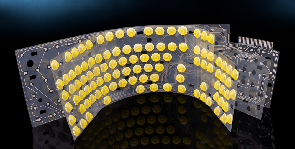
The Custom Keyboard PCB
Custom keyboard PCBs are usually bespoke—not mass-produced. And one unique feature of these custom keyboard PCBs is their programmable feature. So, you can assign a key to a specific function—based on your preference.
Some custom keyboard PCBs are backlit with LED, while some aren’t. Also, some support the KMAC version 1.4 only. In contrast, some types support the KMAC version 1.4 and 2.0.
Custom PCB Assembly
At WellPCB, we support custom PCB assembling prototyping, which produces top-notch custom prototypes. Thus, our custom PCB assembly comprises weight requirements, customized production processes like die and wire bonding, and deviating PCB measurements.
That’s why we meet specific PCB requirements for rigorous industries like defense, LED lighting, medical, etc.
Custom PCB Design Software
Custom PCB design software is numerous in the market. But for this article, we’ll list the top 5 custom PCB design software.
1. PCB123
2. KiCad EDA
3. OrCAD
4. EAGLE
5. Altium Designer
The Custom PCB Capabilities
We’ve listed a table showing the custom PCB capabilities we can deliver.
-
PCB SpecificationsCustom PCB Capabilities
-
Quantity Requirement:1 – 10,000 and more
-
Layer Count:1 to 40 layers
-
Turnover Time:1 day to 4 weeks
-
Certifications:IPC6012 Class 2-3A / IPC6018 Class 3 MIL-PRF-31032 / MIL-PRF-55110 / ISO 9001:2008 / AS9100C / Others
-
Plating Finish:Soft Gold / Electrolytic Hard Gold /ENIG/Nickel/Immersion Silver OSP/Leaded & Lead-Free HAL
-
Materials:Polyimide /Rogers/ FR-4/Aluminum Clad/High-Temp. FR4/Others
-
Trace :Down to 2.75 / 3 Mils
-
Board Thickness:All ranges available
-
Copper Weight:0.5 - 4 oz. Inner / 1 - 20 oz. Outer
-
Legend:Various Color Options
-
Solder Mask (LPI):Various Color Options
-
Rout Tolerance:+/- 0.005 inches (Based on Request)
-
Least Hole Size:0.004 inches
-
Hole Tolerance:+/- 0.003 inches (Based on Request)
-
Plated Holes:Plated / Non-Plated
-
Cutouts:Plated / Non-Plated
Custom PCB Printing: What Does It Cost to Build a Custom PCB?
A 2-layer custom PCB goes for $2.50 per square inch, and a 4-layer custom PCB goes for $8 a square inch.