The exciting new RF front-end design of high-performance radio-frequency (RF) transceivers ensures the best persuasive technology. Generally speaking, if you plan to improve it only by increasing the transistor width or power supply voltage, it will create designing problems. You may need a larger size of PCBs, and there will be more power consumption. In this article, we will introduce tips for the design structure of a low-noise amplifier (LNA) for RF receivers/transceivers.
We will help you produce LNA PCBs which give maximum performance by operating at low power.
Contents
- 1 Design Low Noise Amplifier Circuit with Low Noise Figure
- 2 Calculate Noise Figure and Gain Performance Metrics
- 3 Use the multi-layer Low Noise Amplifier PCB.
- 4 Use Surface Mount Devices in Low Noise Amplifier PCB
- 5 Low- noise Amplifier– Select a Suitable PCB material for Low Noise Amplifier circuit
- 6 Low- noise Amplifier– Design your PCB According to the Requirements of High-frequency Signals
- 7 Achieve Rigid Impedance-matching Circuitry of your Low- noise Amplifier
- 8 Summary
Design Low Noise Amplifier Circuit with Low Noise Figure
It would help if you came up with innovative low noise amplifier schematics to decrease its power and voltage consumption. A low noise amplifier amplifies the antenna’s signal power while making sure that the noise is less. It would supply enough gain to overcome the next stages’ noise.
Generally, an LNA schematic has input and output impedance matching blocks with an amplification block in between them. You should ensure to check the gain constraints of your RF front-end and then minimize the noise figure accordingly. For instance, there can be a constraint that the maximum achievable gain is 20 dB at 2.4 GHz radiofrequency.
We would recommend you to design a linear noise amplifier with inductors. They are reactive, and thus they will not put any noise in your PCB. It is a fact that LC resonance always enhances the noise performance and gain of LNA.

Calculate Noise Figure and Gain Performance Metrics
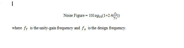
So, we have just told you to keep the noise figure of PCB low. But how can you make sure that it is low? You will need to derive a formula and then do an analysis. Commonly, you will obtain a noise figure and gain performance metrics to check your LNA PCB activity.
Usually, you can calculate the gain of any LNA circuit by deriving a formula that includes load impedance and the transistors’ effective transconductance. For noise figure, you can use the following general formula for analysis:
Use the multi-layer Low Noise Amplifier PCB.
It is important to note that the low noise amplifier PCB would be working at Radio Frequency. Therefore, if you will design a 4-layer PCB layout, it will keep a constant ground plane. It will further permit distributed RF decoupling of a DC power area between two main ground plane layers.
The PCB layout of a low noise amplifier circuit schematic requires a common RF reference point. It is an RF ground point for all the RF signals from an input or output port. By adding a common ground, you will ensure that all the points are at the same potential.
In a 4-layer PCB design, you can set one power plane, two ground planes, and one circuit trace layer. Further, it would help if you adequately designed the shape and width of copper traces. It will decrease the distributed inductance, capacitance, and resistance in the low noise amplifier circuit.

A 4-layer PCB will also permit you to get a manageable size of a microstrip line. A microstrip line is a highly conductive metallic runner on an RF range PCB. You can contact the PCB manufacturer to calculate parameters such as dielectric constant, copper weights, material data, core thickness, and standard layer stack. Using this information, you can effortlessly match the microstrip line to the required impedance value. Finally, it would help if you designed full bias traces to reduce the path resistance.
Use Surface Mount Devices in Low Noise Amplifier PCB
Surface-mount technology is a way in which you directly mount the electrical components on a printed circuit board. If you use surface mount devices, you will get shorter copper traces and smaller noise amplifier PCB sizes. And, in an RF circuit, it will reduce parasitic resistance and capacitance.
Additionally, it would help if you kept the connections between surface mount components and ground short. It is to decrease the impedance. You can also do so by designing two or three parallel vias on the ground plane.
Another critical point is to define the testing temperature range of your low noise amplifier circuit. Your surface mount components must be able to function within this temperature range. Further, you can use banana jacks for bias voltage, ground, and power supply connections. For getting the RF connectivity, you can use SMA connectors in your low noise amplifier PCB. In addition to being small in size, they offer a wide frequency range and high reliability.


Low- noise Amplifier– Select a Suitable PCB material for Low Noise Amplifier circuit
An acceptable PCB material can help the design of your low noise amplifier. It will mitigate the level of heat on amplifier constraints such as noise figure and gain. Altogether, PCB selection can make a significant contribution to the ultimate performance level of your LNA design.
It would help if you considered various PCB material properties as a design candidate for a Low- noise Amplifier. These parameters include dissipation factor (Df), dielectric constant (DK or εr), thermal conductivity, temperature coefficient of Dk, and substrate thickness tolerance.
For instance, you should strictly regulate the Dk of PCB material throughout the material to achieve rigid impedance matching. It would help if you often had it to keep low amplifier noise figures. Moreover, the dielectric constant (Tc Dk) temperature coefficient also affects these noise figures and impedance-matching networks.

Low- noise Amplifier– Design your PCB According to the Requirements of High-frequency Signals
Always remember that you are dealing with high-frequency signals in your small noise amplifier circuit. The PCB will operate in the radio frequency range, so you must design it accordingly. As we have already discussed, it is necessary to use a multi-layer board to reduce interference. A four-layer board’s noise is 20 dB smaller than for a double-panel board with the same material. At the same time, however, there is also a concern that production would be more complicated. The cost would be higher, and you would need the expertise to design the PCB layout.
The RF signals in the low noise amplifier circuit must not develop a loop while wiring. If you cannot avoid it, you can ensure to keep it as small as possible. You should also pay attention to the crosstalk, which can develop at a close distance to parallel signal lines. Crosstalk is the undesirable noise signal among RF signals because of the interference of nearby electromagnetic fields.
There are different methods to avoid crosstalk. You can try to connect the parallel lines in one layer in perpendicular and the different layers. Also, you should use a smaller number of vias in your low noise amplifier design. It will increase speed and decrease data errors. Finally, please keep the wires between the pins shorter. It is to avoid coupling with the components due to longer RF signal leads.

Achieve Rigid Impedance-matching Circuitry of your Low- noise Amplifier
It would help if you tried to get rigid impedance matching circuitry for your low noise amplifier. It accounts for optimal noise performance, filtering and provides input and output stability. Passive elements such as resistors, strip lines, capacitors, and inductors make up the matching circuit.
The PCB material tolerances such as copper thickness and conductor width tolerances influence this circuitry. If there are any problems related to circuit fabrication, it will also influence your impedance matching circuits. The size of these tolerances depends on the specific design of the LNA system.
For instance, copper thickness tolerance has a more significant impact on coupling structures, like coplanar circuits.
On the other hand, the influence on the substrate’s circuit conductor width and thickness is concerned. Thinner channels display more significant impedance adjustment than thicker courses for an increase in conductor width.
DK tolerance is another parameter for PCB, which may influence your impedance matching networks required in LNA designs.

Summary
So, these are some tips that you can follow to design your low noise amplifier circuit correctly. You need the right impedance matching networks, PCB material, PCB layers, bias circuits, noise figure, and gain. You can ensure a quality design by designing your low noise amplifier PCB according to RF frequency signals requirements.
If you need correct PCB service provider. Thankfully, there are various PCB manufacturing services, you can contact us, and we can provide technology, materials, and quality services. Contact us now.