Contents
1. Bluetooth technology
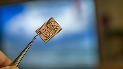
The Bluetooth circuit consists of several PCBs with multiple components such as diodes, resistors, and capacitors.
The PCB may be assembled in two layers on both sides of the plate.
The chip processes the signals fetched from the antenna and generates an output.
Note that the presence of a PCB close to the antenna may lower the resonance frequency, so it is recommended that the thickness of the PCBs used in Bluetooth be about 1.6 mm.
It is also recommended that you don’t place any metal, including copper, anywhere near the area marked GND; the GND pins must be connected to the plane.
Switching the vias could avoid any emissions from the PCB. A Bluetooth connection allows the transfer of stereo signals from the two wireless devices.
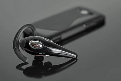
The headset will bridge and deliver audio signals to the two devices.
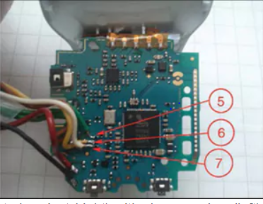
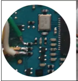
A few wires must be soldered to the PCB to allow signal transmission and ensure smooth sign transmission.
Typically, the PCB is soldered at the bottom of the enclosure.
It can be observed by opening the front cover and removing the plastic section depending on the design of the PCB.
2. Assembling A PCB Wireless Bluetooth.
To assemble Bluetooth, a different layout could be used. However, it would help with a Bluetooth headstart, switches, amplifiers, LEDs, and an enclosure.
Ensuring that cables do not cross the headstart is essential since it reduces Bluetooth range.
Also, the system should not be placed near transmitters because they impact and affect transmission.
Once all the required components have been assembled, you should solder wires, and the LEDs soldier the on and off wire onto the headset’s PCB.
Designing the PCB to be used in your Bluetooth stereo is possible.
First, you must choose the PCB design you are interested in.
You also need to determine the number of layers you need.
More layers are needed for Bluetooth.
You should then assemble the following materials: epoxy, cotton paper, and epoxy.

3. Designing the Bluetooth PCB
First, you need to develop a schematic that includes all the components you will need. You can use software to help you create a schematic.
After selecting the tool, you should get the right components according to your schematic diagram.
Contact the specification of the element from the vendor’s website. Follow the datasheet and connect the lines to the relevant details.
Place the components on the schematic, and you will be ready.
Note that the success of your project depends on the schematic diagram you come up with.
It will be a source of reference and will form the point of communication with your engineers.
Place the components on your PCB and connect them between the layers.
The PCB should be divided into sections depending on its functionality.
It helps you to keep the conductive traces short.
This is critical, especially to reduce interference and the conductive path.
The user interface is critical and should be considered when designing your Bluetooth PCB. As you work on your PCB, consider components such as connectors, jacks, and LEDs.
Once you create the layout, produce a Gerber file and send it to the PCB manufacturing company to make your PCB.
Your PCB manufacturer will print the circuit after they have verified that your design is not faulty.
The manufacturer should help you source the components you indicated you would use to make your Bluetooth.
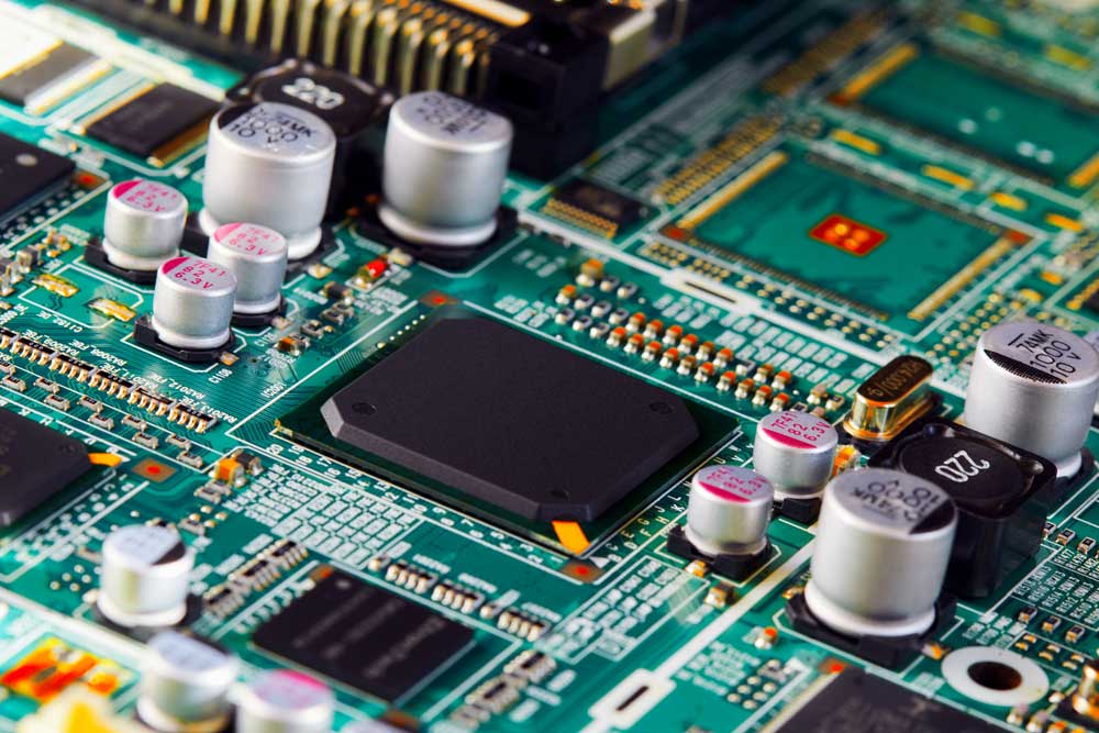
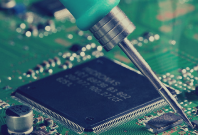
4. Mounting the Components
It is placing components into the holes on the surface of your PCB, as shown below.
To do this successfully, you need to remember a few things:
First, check the component’s type number and try consolidating them to optimize their use.
Once you finish the placement, you can solder them by reflowing.
You may use an infrared lamp or an oven to do this job.
Once the solder melts, it will permanently connect the components on the board.
If there are components that the machine cannot mount, it should be done manually.