
A Bluetooth circuit is the central part of Bluetooth and contains components such as the integrated circuit, capacitors, and power source. The course supports wired-in audio, wireless stereo, Bluetooth module, and many more.
The IC contains a charger and voltage regulator. The Bluetooth module includes information on the configuration and the setting.
The Bluetooth connection operates in the 2.4 GHz range. In the operation of Bluetooth devices, the primary device can be called the controller device, which is then connected to other mini devices often referred to as ‘slaves.’
Now, please follow me to learn more about Bluetooth circuits.
Contents
Bluetooth Circuit
1.1 Definition
With the advancements made every day in the technology niche, life becomes more accessible and more comfortable since most human needs have gotten solutions through technology.
Bluetooth technology is yet another advancement that has made communication between devices seamless.
The Bluetooth technology is a significant advancement from the legendary wires and cables that have been the most used method of communication between or among devices.
The other form that has been used for communication devices is the application of radio signals, infrared signals, and wireless technology.
The Bluetooth technology is an advancement from the previous infrared technology. In infrared radiation technology, you could only connect two devices simultaneously, thus posing a significant disadvantage.
With Bluetooth connectivity, you can connect multiple devices at the same time and transmit data too.
One example of the application of infrared technology is the remote control system.
The remote control system works by what is popularly known as the ‘line of sight technology,’ which means you must point the remote at the target for it to work.
This kind of technology is limited and thus reduces the applications and uses in different areas. The Bluetooth connectivity is other because it can be used anywhere so long as you are in the range of the radio signals that it utilizes.
A Bluetooth circuit, therefore, works by the use of radio signals. In most cases, the frequency that has been set aside for Bluetooth connectivity is 2.4 GHz. However, this is not entirely the case as other devices also use this frequency, posing a possible interference.
Luckily, the Bluetooth circuit uses low power signals to avoid any interruption from the other devices due to technological advancements. Therefore, that is why most Bluetooth devices only work within a range of 10 meters, out of which the connection can be lost.
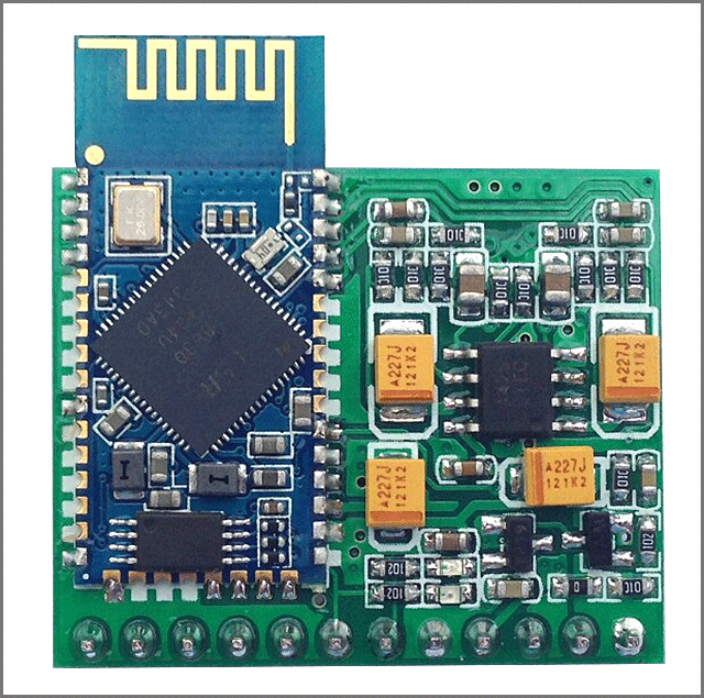
The Bluetooth circuit consists of several PCBs with multiple components such as diodes, resistors, and capacitors. The PCB may be assembled in two layers on both sides of the plate. The chip processes the signals fetched from the antenna then generates an output.
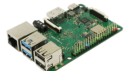
1.2 Bluetooth Circuit Board
A complete Bluetooth circuit board must contain an antenna that helps to send and receive information. A Bluetooth circuitry must include at least two inductors whose job is to fine-tune the antenna’s impedance to enhance performance.
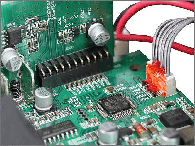
There is also another secondary circuit board located inside the speaker. It connects the audio line, power button, and USB power. The secondary board comes with two LEDs.

1.3 Bluetooth PCB
Bluetooth PCB technology is a communication technology that operates at a range of 2.4GHz. It is a radio frequency range that makes use of Wi-Fi technology.
The Bluetooth communication has a master device that is remotely connected to a maximum of seven slave devices. It covers a distance of 10m max.
Bluetooth devices communicate by exchanging unique codes and so will only work if there is approval from the other user.
The presence of a PCB close to the antenna may lower the resonance frequency. And so, it is recommended that the thickness of the PCBs used in Bluetooth should be about 1,6mm.
It is also recommended that you don’t place any metal, including copper, anywhere near the area marked GND and the GND pins need to be connected to the plane. Switching the vias could be done to avoid any emissions from the PCB.
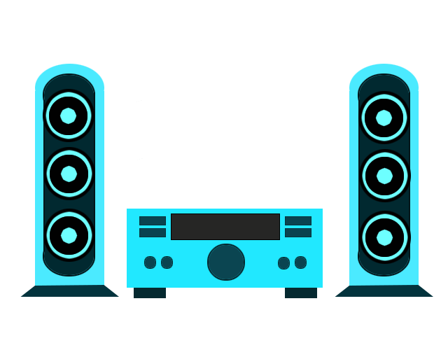
A Bluetooth connection allows the transferring of stereo signals from the two wireless devices. The headset will act as a bridge and deliver audio signals to the two devices for smooth movements. A few wires must be soldered to the PCB to allow for signal transmission.
The PCB is soldered at the bottom of the enclosure. It can be observed by opening the front cover and removing the plastic section depending on the design of the PCB.
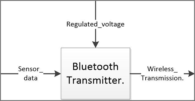
Bluetooth Transmitter Circuit
A Bluetooth transmitter circuit facilitates the transmission of music to the stereo. It also enables the pairing of your Bluetooth with other devices to allow you to enjoy wireless music. The circuit must have a charging system and a recyclable battery.
The transmitter circuit contains some components, including LED indicators. The course allows the transmitter to connect to your device immediately after it is switched on.
It is also designed so that it can be in standby mode until a request is sent to the transmitter.
The recyclable battery that is found in a Bluetooth transmitter circuit can last for a period of up to 10 hours. In such a case, a lithium battery is most preferred since it is long-lasting.
It ensures that you can listen to the music over an extended period without the battery running out.
The cell contains a small circuit whose purpose is to protect it from over-current, over-discharge, over-charge voltage, and short course.
Notice that the services offered by the speaker are handled in the main primary circuit board. The circuit board section consists of voltage regulation, battery charging, Bluetooth, and audio amplification.
You will get a microphone with volume up/down /pause control at the end of the board.

Bluetooth Circuit Board Kit
The Bluetooth circuit has a board kit that ensures you effectively play music or any other content from your phone. That achieved wirelessly through advanced technology.
The Bluetooth circuit board is available in three formats:
- As a single entity.
- With 65mm speakers.
- With 100mm speakers.
The Bluetooth circuit board ensures seamless audio quality and connectivity, a vital part of Bluetooth devices. It is the central part that controls the entire machine.
Without this kit, the connectivity and complete functionality of the Bluetooth device would be paralyzed.
It is light in weight, thus being advantageous in the sense of manufacturing different devices.
That means that whichever appliance you decide to design, you can easily incorporate the Bluetooth circuit board kit. It is used in both small and large devices.
The interface for the circuit board kit is easy and straight to the point. The design of this kit is in such a manner that it tries to connect to the last device that it was paired to whenever the Bluetooth in the device is turned on again.
In cases where the device was last paired to be off or not available, the Bluetooth circuit board kit is programmed to try and match with another device that is close to it or within its range.
The Bluetooth circuit board kit can be powered using two types of batteries
You can either use the 1A USB supply or LiPo battery. The board is also made with sounds and LED lights that would indicate the status of the Bluetooth connectivity.
Some of the features of this circuit board kit include the following:
- LED lights and sounds that may indicate the state of the Bluetooth connectivity.
- Enables devices to play content seamlessly through wireless connectivity.
- It is programmed to have a simple user interface that the user can quickly use. The design is such that you only have to use the on/off button to operate.
- It is designed to reconnect to the last paired device or pair to the closest device within range.
Bluetooth Audio Circuit
4.1 Bluetooth Audio Circuit Feature/Usage/ How to make and use
The Bluetooth audio circuit consists of the speaker, typically constructed by melting the plastics to form the perforated grills. The course comprises two speakers and a battery.
The battery has a circuit board that protects it from over-charge voltage, over-discharge, and overcurrent. It also contains an audio amplifier, which supports two outputs.
It also consists of the 4558 Op- Amp.
Designing a Bluetooth circuit starts at the circuit design level. The design of the course depends on where the channel is to be applied.
For instance, Bluetooth for low energy products should feature magnetometer, accelerometer, gyroscope, and sensors that measure temperature and humidity.
To construct the circuit, all you need is a Bluetooth Low Energy microcontroller, a crystal oscillator, tunable load capacitors, and a 24 MHz crystal.
You also require power pins, an IC, and a capacitor.
It would help if you also had a clean, stable voltage and power supply capacitor to filter and stabilize the power.
May make use of a decoupling capacitor and a storage reservoir with a low impedance.
Note that to achieve a low impedance, it may require that you place a 1.0μF in parallel. A ferrite bead may also be included.
4.2 How To Make A Bluetooth Device Circuit
In making a Bluetooth circuit, you would need to start by creating a schematic for the course. In coming up with the schematic, you may need to use the software.
According to your schema, you can then get the necessary components that will help you complete the circuit.
After that, you can connect the components following the lines in the schematic diagram you have.
Your project can only succeed if you have the correct schematic diagram.
It shows the importance of the schematic.
One other thing that you need to factor in when making the Bluetooth circuit is the user interface. The Bluetooth circuit is all about the user and how they will use it to achieve their needs.
You need to produce a Gerber file after you are done which you can then send to the manufacturing company for the Printed Circuit Board of the device.
After verification of the design, the manufacturer then prints the circuit board.
Different types of devices utilize the Bluetooth technology. Generally, the headsets use smaller speakers.
The PCB layout is the most challenging part for starters. If you can create the design for the PCB, then you are good to go.
Different layouts could be used to assemble a Bluetooth circuit; however, you need to have a Bluetooth head start, switches, amplifiers, LEDs, and an enclosure.
Ensuring that cables do not cross the head start is essential since it reduces Bluetooth range.
Also, the system should not be placed anywhere near transmitters because they impact and affect transmission.
Once all the required components have been assembled, you should then solder wires, and the LEDs soldier the on and off wire onto the headset’s PCB.
Notice that it is possible to design the PCB to be used in your Bluetooth stereo. First, you need to choose the PCBs design that you are interested in.
You also need to determine the number of layers that you need to have.
For Bluetooth, you need to have more layers. You should then assemble the following materials: epoxy, cotton paper, and epoxy.

When mounting the components, check the components type number and consolidate them to optimize their use. Once you are through with the placement, you can solder them by reflowing. You may use the infrared lamp or an oven to do this job.
Once the solder melts, it will permanently connect the components on the board. If there are components that the machine cannot mount, it should be done manually.
Conclusion
The Bluetooth circuit is simple to design and make type of circuit and requires only a bit of experience to come up with. The course is responsible for the connectivity of devices that would utilize the technology.
Many devices utilize Bluetooth technology nowadays for different purposes, and this is due to the convenience it brings along.
You can come up with the Bluetooth circuit using DIY methods, but if you are not very sure of what to do, it is better to use an experienced manufacturer.
In case of any inquiries, you can contact us.