contact
3rd Floor, Nanhai Plaza, NO. 505 Xinhua Road Xinhua District, Shijiazhuang Hebei China
+86-311-86935221
+61-0417-264-974
[email protected]

Electronics Manufacturing

  • PCB Manufacturing and assembly industry are one of the most important parts of electronics manufacturing.
  • Contact us to get to know more about WellPCB PCB manufacturing and assembly do in electronic development.

PCB Manufacturing
Capabilities

WellPCB is a reputable and professional PCB manufacturing and assembling company with roots in China. The table below shows some of the primary capacities that we provide and support. It contains information about the PCB materials we use, the PCB technologies we leverage, the types of products we manufacture, and our offer’s tolerances.

  • Materials:
    FR4, High TG FR4, Halogen Free Material, CEM-3, Rogers HF Material
  • Min. Contour Tolerance:
    + / -0.1mm
  • Layer Counts:
    2-36 Layers
  • Min. Finished Diameter of PTH Hole:
    + / -0.1mm
  • Finished Copper Thickness:
    0.5-5 OZ
  • Max.Board Thickness/Hole Ratio:
    12:1
  • Finished Board Thickness:
    0.2-6.0mm
  • Min. Solder Mask Bridge:
    4mil (Min, SMT Pad Space 8mil)
  • Min.Line/Track Width:
    3mil
  • Min.Legend(Silkscreen) Track Width:
    5mil
  • MIN.Drilling Slot Size:
    0.6mm
  • Surface Treatment:
    Leaded HASL, Lead Free HASL, Immersion Gold, OSP, Immersion tin, Immersion Silver, etc.
  • Solder Mask Color:
    Green, Black, Blue, White, Yellow, and Matt, etc.
  • Other Technology:
    Gold Finger, Peelable Mask, Non-across Blindried Vias, Characteristic Impedance Control, Rigid-flex Board, etc.
  • Solder Mask Hardness:
    6H
  • Legend/Silkscreen Color:
    Black, White, Yellow, and others.
  • Wrap and Twist:
    ≤0.7%
  • Flammability:
    94v-0

The PCB Manufacturing
Process

why us

Since 2007, WellPCB has offered good-quality PCBs with excellent turnaround time and customer satisfaction. We are one of the biggest and most skilled board manufacturers in China. Our committed staff- with a rich experience in the electronic world- produce superior products, such as double-sided, single-sided, multilayer, and HDI PCBs.

PCB & PCBA One-Stop Service

  • We offer in-house PCB manufacturing.
  • We procure original and authentic PCB materials.
  • We procure components from authorized suppliers
  • We offer stencil and assembly services

Unbeatable Prices on PCB Products

  • We offer one of the most competitive prices in the PCB manufacturing world.
  • We have our factories with genuine cost control and no hidden charges.
  • We support numerous payment methods, such as T/T, credit card, PayPal, bank transfers, etc.
  • Our factories offer price support for different orders, especially for multilayer boards and mass production.

On-Time Delivery

  • Our main delivery channels are DHL, FedEx, and door-to-door services. Typically, shipping takes 2-4 days.
  • We have developed a good relationship with the major shipping companies, and they offer discounts to us.
  • We provide Anti-static + Moisture-Proof + Anti-Vibration Packaging and Inspection Certificates.

Quality Assurance

  • Our products adhere to the IPC and the ROHS and REACH Standards.
  • We boast of over 99% customer satisfaction rates.
  • We have standardized factory processes and management.
  • We pass our products through multiple testing procedures.

Excellent Customer Service

  • We offer instant online quoting and ordering services.
  • We guarantee quality in our services.
  • We have unbeatable prices and offers, and we do not require a minimum order quantity.s.
  • We have a 24/7 and experienced support team available via online, phone, and email.

Return and Refund Services

  • In case of any severe default in our products, you can request compensation or a refund.
  • We refund directly to your preferred payment method. We can also rework or refabricate the product and reship it at our expense.

Rigorous Quality Control System

  • We operate strictly in line with international quality standards, guaranteeing 100% shipment quality.
  • Our thorough inspection procedures warrant high PCB dependability and stability.

Professional Technical Team

  • We are a one-stop PCB manufacturing and service provider offering customized, fast, and high-end products.
  • We pride ourselves in decades of PCB production, offering optimized printed circuit boards worldwide.
  • We have hired top-cream personnel with rich experience in standard PCB fabrication and advanced PCB fabrication.

Previous slide
Next slide

PCB Factory Scale

We handle all production scales, including small, medium, and mass production orders.

Besides, we can deliver more than 10,000 products monthly.

We have competitive prices and unbeatable offers for volumes ranging from as small as 1 square meter for you.

Our Certifications

Here are the certificates we have:
IATF 16949:2016 ISO 9001:2015 ISO14001:2015 ISO13485:2016 UL Also, all our products follow the IPC & ROHS Standards. More importantly, we always strive to manufacture high-end PCB products.

PCB Product Show

Custom PCB Packaging and Shipping

Testimonial

NXP France

Top Questions

1. What services do you offer?

We offer three primary PCB assembly services: PCB fabrication, consigned PCB assembly and full turnkey services.

2. Is it possible to get stack-up drawings from you?

Yes, we are willing and ready to share some of our standard stack-up drawings with you, or even individual stack-up drawings that meet your specific requirements.

3. Do you offer any discounts?

Our two factories offer price support for various orders, especially for multilayer PCBs and mass production.

4. Can you view and process Altium CAD data directly?

Unfortunately no. We generally deal with Gerber files.

5. What if I am dissatisfied with PCBs from WELLPCB.com?

If you encounter any problem with our products or feel dissatisfied with our products or services, you can let us know through [email protected]. We promise to get back to you within 24 hours and serve you satisfactorily. We will either refabricate your PCB in case of a defect or refund the full amount without needing to return the defective PCBs. You may also choose to credit your[email protected] account and use the credit for future orders.

PCB Creation-How To Create Your PCB

Table of Contents

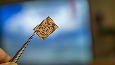
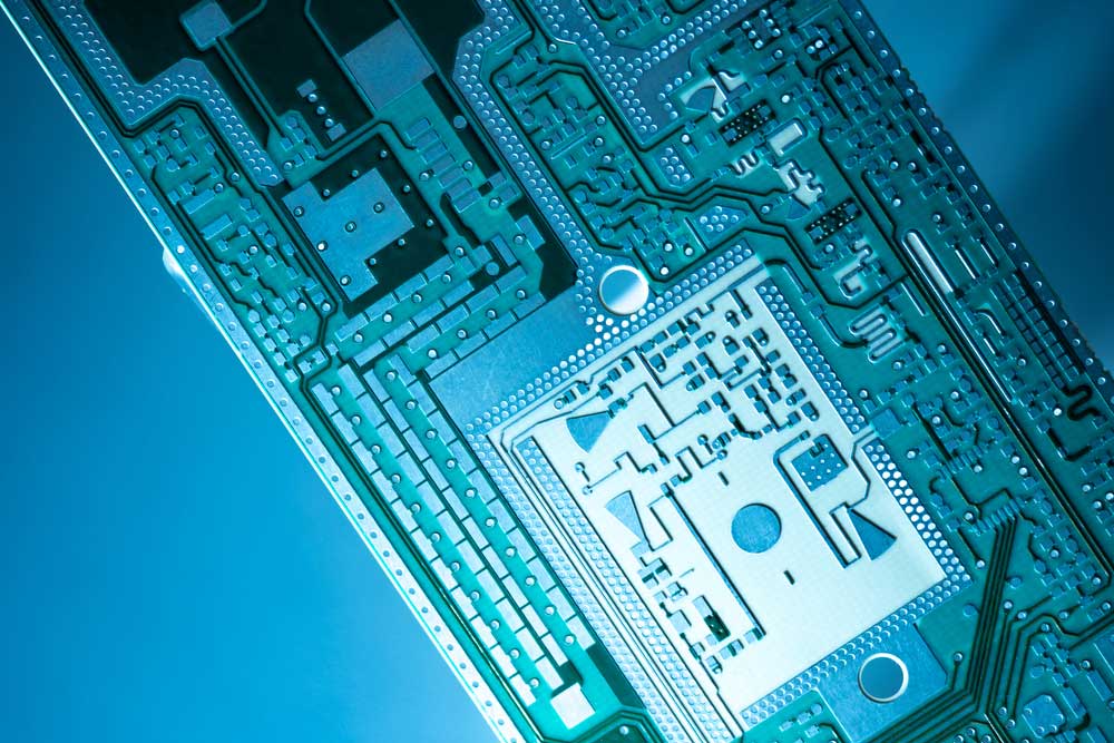
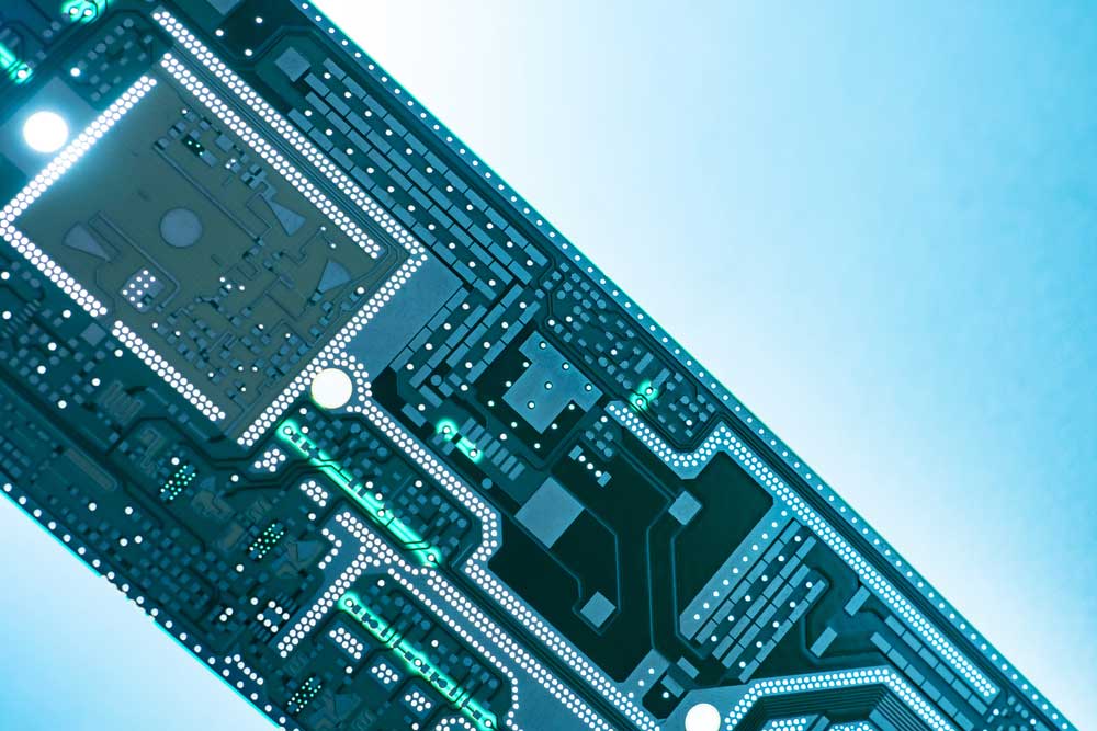
PCB creation is a simple process that can be carried out even at home. Creating your board reduces the cost and eliminates problems that arise from loose wires in your circuit. Flexible cables are always associated with accidents as a result of short-circuiting.

1.Why We Should Learn To Create Our Own PCBs At Home

Creating the boards at home is economical as it reduces the cost and the number of loose wires in your devices. If properly designed, it reduces the size of the devices and may help make your connections secure.

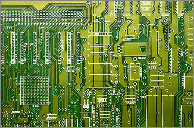
Typically, a printed circuit board supports and connects components using pads and tracks. It has predesigned copper tracks which connect different parts of the board and thus eliminate the use of wires. It reduces faults associated with loose connections.

PCB Creation1.png

Steps to Creating PCBs At Home.

Pcb creation will help you save time and money. The trouble is that most of us may not know how to do this. Here are steps to guide you when you choose to create your PCB at home.
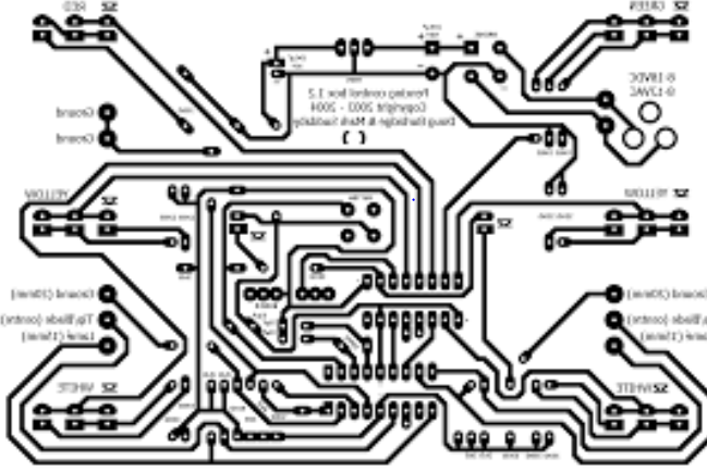
2.PCB CreationPCB Creation Design

It is the first step towards PCB Creation. It entails converting the schematic diagram into a PCB layout. Software may be used for this purpose. Among the software that you can use include PCB wizard and Cadsoft Eagle.

3.Designing Schematic in Cadsoft Eagle

Materials

It would help with an etching solution, a blade cutter, glossy paper, cotton wool, sandpaper, and a black marker.

PCB Creation2.png

PCB Creation–Procedure    

1.Use a laser printer to print out your PCB layout.

2.Select an appropriate PCB design software and make the printout on a piece of paper.

3.Using the blade, cut out the copper board to size using a hacksaw.

4.Use steel wool to rub the copper side of the board to remove the copper oxide layer. It allows the paper image to stick.

5.Transfer the PCB print onto the plate by placing the photo paper on the board and putting the copper surface on the printed layout. Check and ensure that the board is well aligned with the printed form. You may use tape to secure the printed paper in position.

6.The printed side of the paper should then be placed on a board to allow you to trace the circuit using a black marker.  

You may use a copper iron to do this job. Ensure that it is heated to maximum temperature before transferring the image onto the plate. 7.Iron the printed circuit onto the PCB plate by ironing the image on one of the sides. As you do this, you need to pay attention to the edges and ensure that they are well aligned before transferring the image onto the plate.

8.When transferring the image onto the plate, it is recommended that you use a long hard press and desist from moving the iron as it is done when ironing clothes. A hard press will transfer the ink from the paper to your copper plate. Finally, place the printed container in water and wait for it to dissolve before peeling it out gently.

PCB Creation3.png

Circuit Board Fabrication and PCB Assembly Turnkey Services

Online Quote Contact Us