Contents
- 1 What are the PCB Layers?
- 2 Single Layer PCBs vs 2 Layer PCBs vs Multi-Layer PCB (4 Layer PCBs/ 6 Layers PCB)
- 3 How to Know the Number of Layers in a PCB?
- 4 Types of PCB Board Layers / How Do PCB Layers Work?
- 5 Rules: Keep Out and Routing Layers
- 6 The Terms and Concepts Used in Printed Circuit Boards
- 7 Closing Words
What are the PCB Layers?
First, before we dive deeper into PCB layers, let’s start with a clear understanding of what “layers” mean. These layers are essential in assembling or building a PCB.
A layer is a signal-conducting level oriented vertically to the PCB plane. For example, in a 2-layer PCB, you’ll have both a top and bottom layer. In a 4-layer PCB, you’ll typically find a top, inner 1, inner 2, and bottom layer.
This structure applies similarly to PCBs with more layers, enabling complex designs and functionality. If you’re considering advanced configurations, PCB production with additional layers might be the right solution for your project.
But that’s not all.
Each PCB layer contains an insulated substrate. Typically, this substrate is FR4 (Fire Retardant Version 4), a material made of epoxy-saturated fiberglass adhered to a tough copper sheet, often prepared before the etching of the circuit pattern. For RF boards, however, substrates are generally Teflon-based to support high-frequency applications.
In standard PCBs, solder masks cover the outer copper layers and can be found on both the top and bottom layers. These solder masks are applied as either a liquid or a sheet, with printed openings created through a subtractive photographic process.
When working with a specialized flex PCB manufacturer, you gain access to the expertise needed to select and apply appropriate substrates and solder masks, ensuring your PCB design meets specific performance and durability standards.
Let’s face it, PCB layers are the foundation blocks of a PCB. So, they include the copper, the dielectric material, and one more thing. And it’s the trace dimensions aligned with the dimension or mechanical layer.
So, let’s talk about each piece.
Dielectric Materials
The dielectric materials offer two critical functions for PCBs. And all that happens as the PCBs run rapid signals.
1. The dielectric materials help to isolate signals on adjacent PCB layers.
2. The stability of a PCB highly depends on the steady impedance of dielectric materials. And it’s usually over the whole plane. Also, it monitors the constant impedance over an extensive frequency range.
Copper
The function of copper in a PCB is pretty apparent. Every engineer knows it acts as a great conductor. But other vital functions exist.
The various weights and thicknesses of copper in a PCB impact too. Of course, it influences the capacity of the PCB to attain the right amount of current flow. Also, it helps to describe the amount of current loss.
But that’s not all.
The quality of copper in a PCB impacts the impedance of a ground plane. Plus, it affects the power plane’s thermal conductivity.
Furthermore, merging the copper’s length and thickness helps to do something. Mainly for different signal pairs, it solidifies the PCB stability. It also does an excellent job of the circuit’s integrity. And it’s even better if it’s for high-frequency signals.
Trace Dimensions
Dimension lines and markings have their uses in a PCB. Of course, their obvious function is to describe the dimension and mechanical layer.
But that’s not all they do.
They also help to provide PCB foundational measurements. Plus, the assembly information helps to regulate the location and mounting of electronic devices.
Also, the assembly process entails that design teams focus on the following. So, the design teams must focus on thermal, signal management, etc. Plus, the pad placement isn’t left out. They should also know the difference between mechanical and electrical assembly rules.
Designers must also check if the physical component mounting reaches its mechanical requirements. So, designers need this info because the PCB connects functional parts to PCB traces.
In the long run, all PCB design layers require assembly documentation. Plus, there are other documents like Gerber data, the schematic, BOM, CAD data, etc. Plus, wne have fabrication drawings, assembly drawings, notes, quality, and test specifications.
Single Layer PCBs vs 2 Layer PCBs vs Multi-Layer PCB (4 Layer PCBs/ 6 Layers PCB)
The three most common PCB layers are as follows:
1. Single-layer PCBs or 1-layer PCBs.
2. Double-layer PCBs or 2-layer PCBs.
3. Multi-layer PCBs or 4-layer PCBs.
However, layer PCBs have their differences. Also, engineers use them for PCB manufacturing in specific situations. That’s what we’ll dwell on in this section.
Single Layer PCB (1 Layer PCB) And Double Layer PCB
Single-layer PCB comes with only one conductive layer material. Plus, it’s ideal for simple designs and low density.
In comparison, double-layer PCBs come with two conductive layer materials. Also, it has a larger surface area. Plus, it houses a conductor pattern. And its surface area is twice the size of the single layer.
So, if you’re a student or hobbyist, you should opt for the single layer. And it’s because the single layer is simpler to create. In contrast, Double PCB layers are quite hard to produce. But if you insist on using the double-layer PCB, you can buy it from a commercial producer.
Double Layer PCB And Multiple Layer PCB
Engineers use the double-layer PCB more than the multiple-layer PCB. And the reason is that it houses interconnects on two sides. However, the multiple-layer PCBs’ strength is its interference level and signal integrity.
Thus, we’re going to look closely at their differences. Also, we’d take the 4-layer PCB as an example in this post. And we’ll use four key factors. So, they are as follows:
Designs
The 2-layer PCB involves the creation of electrical connections. These electrical connections allow the routing of traces. By doing so, current traces reach both sides of the PCB.
In comparison, there are more current traces for the multiple (4-layer) PCB. And it’s because it has a larger surface area.
Also, the multiple (4-layer) PCB uses a prepreg layer. Hence, it bonds double-sided boards with two layers. It does this by applying pressure and heat. Plus, the prepreg offers dielectric between the layers.
PCB Layer Stackup
The 2-layer PCB stack-up comes with one top and bottom layer. But the multiple (4-layer) PCB doesn’t have just one top and bottom layer. It also has two inner layers. They are inner layer one and inner layer 2. Plus, there’s a prepreg between inner layer one and inner layer 2.
Functionality
When it comes to microstrip traces having a ground plane, something happens. The 2 Layer PCB brings more functionality than the multiple (4 Layer). And it’s because it doesn’t face any propagation delays or issues.
Besides, the multiple (4-layer) PCB consists of VCC and ground plane layers. The 4-layer design has propagation delays and impedance issues.
Cost
The 2-layer PCB is more affordable than the multiple (4-layer) PCB. And it’s because the 4-layer PCB has more complexity.
Lead Time
The lead time is the amount of time required for a producer to create a PCB layer. So, whether it’s single or multiple layers, you need to consider it before making orders for printed circuit boards.
The lead time for a 2-layer PCB is usually within one. However, it all depends on the surface area of the intended board. But then again, you can get the 2 Layer PCB in 5 days, if you’re willing to pay more for expedited cost.
For the multiple Layers like the 4 Layer PCB, it takes about 12 – 32 days delivery time. But once again, the delivery time also depends on whether you want large or small board dimensions.
How to Know the Number of Layers in a PCB?
Here are the steps that will guide you through picking the number of layers you need in a PCB.
Step 1: Determine the Number of Layers You Want
There are a different number of layers. They include the following:
1 or 2 Layer PCBs
It’s best to opt for this option if you want a very simple board. Also, it’s useful for some breakouts. But, it’s not ideal to use this type of layer PCB for interfaces that have controlled impedance.
4 Layer PCB
They are one of the safest options to pick. Also, this layer PCB is ideal for small boards, breakouts, and simple boards. Also, you can use the four-layer PCB for some microcontroller boards and Base Boards.
But, you should avoid this type of PCB layer for CPU boards escorted by a memory interface.
6 Layer PCB
If you plan on dealing with large boards, the six-layer PCB is ideal. Also, this layer PCB is a good option if you’ll work with many boards. After all, you’ll find a few PC motherboards built on six Layer PCBs.
8 Layer PCB
Generally, the 8-layer PCB is ideal for compact devices with restricted spacing. So, you can find them installed in wearable watches, PC motherboards, communication backplanes,etc. Also, 8 Layer PCB usually offers more planes for shielding signals on adjoining layers.
10 Layer PCB
The ten-layer PCB is the highest number of layers you can use—to fit into a 1mm thick SODIMM socket. Plus, this layer PCB has plenty of room for power planes. And it comes with a lot of power domains.
12 Layer PCB
Suppose you deal with many industrial designs; it would be best to consider twelve-layer PCBs. Also, this layer PCB goes for a reasonable price. Plus, this layer PCB has four solid ground planes. And it has two extra signal layers.
Begin With the Layout
When it comes to the layout, it’s best, to begin with, the bottom and top layers. And if you notice that your design leverages high-speed signals, combine two extra inner signal layers. You can also apply this method if your system has too many connections.
Before you start with the layout, ensure that you place it all into the signal layers.
What if you require more space in the process? It’s best to combine your power plane layers with slow signals. But if you require much space, you can add extra signal layers (two preferably).
Place Your PCB Layer in Order
There are plenty of options when it comes to placing the PCB layers in order. You can utilize GND as the secondary layer. And it’s because it acts as a reliable shield against high-speed signals dashing inside the PCB.
Find out the Signal Layers and Density Required
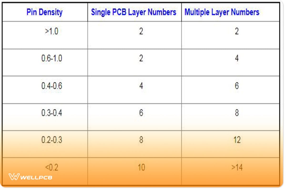
To know the number of layers, you need to also determine the required density and signal layers. So, we’re going to show how it works in the below chart. If you look closely, you’ll notice that a 1.0 pin density will require two single layers. Thus, the number of required layers rises as the pin density reduces. Also, with a lower pin density of say 0.2 or even less, you’ll need a minimum of 10 PCB layers.
Here’s the chart below.
Types of PCB Board Layers / How Do PCB Layers Work?
Now, you know how to determine the number of layers you need for your project. The next step is to understand the types of PCB layers. They are:
Mechanical Layer
The function of a mechanical layer is to reveal information about the PCB assembly methods and printing. So, you can choose to have more than one mechanical layer. But, it’s crucial to note that you’ll require one mechanical layer to fabricate your board.
You can also use Mechanical 1, which is a basic layer to plan your board’s dimensions. While you’re at it, the fabricator will use the basic layer to get your circuit board from the stock material.
Your cut-out can be a complicated shape or a simple rectangle. Also, you can choose to add more mechanical layers.
Overlay / Silkscreen Layers
The Silkscreen layer consists of the Bottom and Top overlay. And it’s useful for putting text information. But, if you’re using this layer, it’s crucial to get separate files, for the fabricator, to the bottom and top overlays.
You can also decide not to use these layers internally. After all, you won’t be able to see them. But, you can avoid this layer totally if you don’t want any text on your board.
On the other hand, it’s best to use this layer since they are useful for debugging boards in the lab. You can also use this layer to add your board’s serial number, company name, revision number, etc.
What if you plan to include your serial and revision number later?
Well, you can print blank boxes for this information. Then, use a sharpie or stamp to write the numbers on the board.
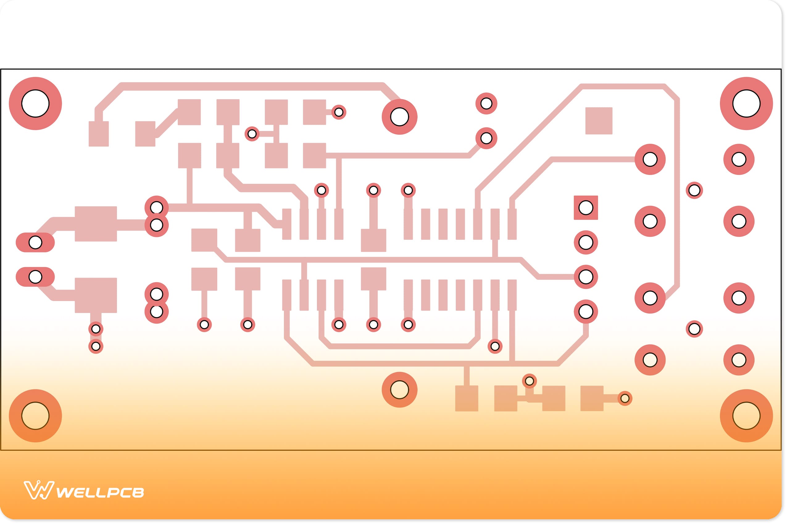
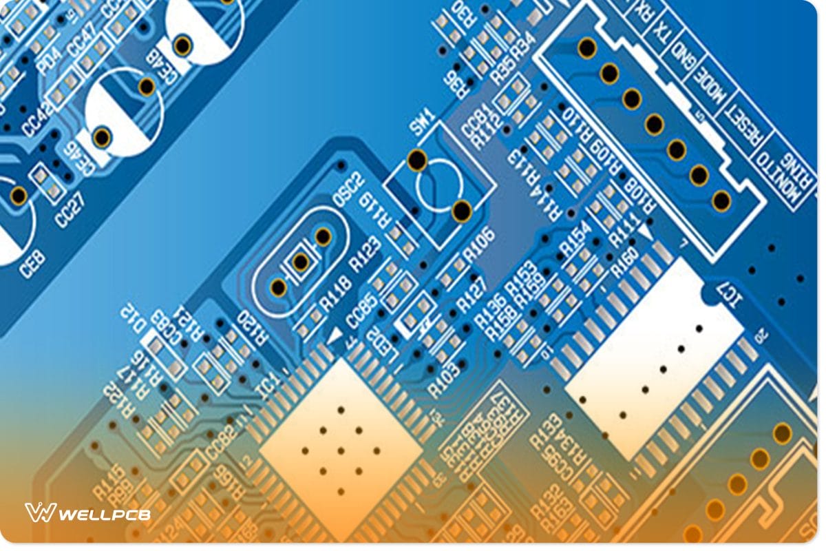
Routing Layers
You can find routing layers in the internal and external parts of a PCB. Also, it’s a layer that designers take time to perfect. Plus, it’s useful for component interconnection. Before you create your board, it’s necessary to provide the routing layers to your fabricator.
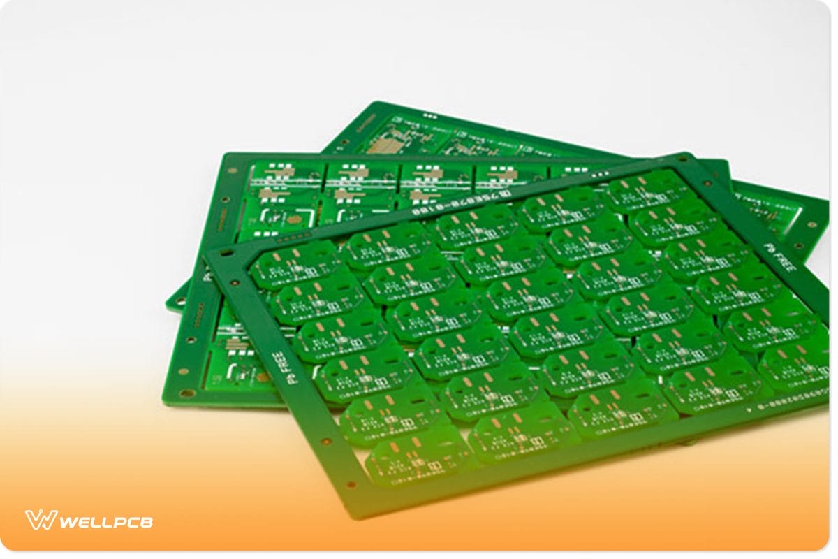
Solder Mask Layers
A solder mask layer is what you see when you hold a PCB. That is, it’s a thin green protective covering. And it usually helps to cover the board’s top and bottom. If there’s debris on your board, this board will help you protect traces from shorting.
If you use this layer, it’s crucial to provide the files for the parts where the layer covers. Plus, you have to specify the information on this layer as negatives. In other words, you have to consider areas you won’t cover with the solder mask layer. And you’ll fill in on this layer.
For instance, you can’t use the solder mask layer on an area where you’ll add components to make electrical circuit board shopping, various things might get you confused. Whether you are going for a single-sided PCB, a double-sided PCB, or any other type of PCB, You can contact with your PCB.
Solder Paste Layers
A solder paste comes in handy when you have surface mount components. So, this layer helps to bond the component pin to the surface (copper) of your board. Also, it improves the flow of the solder.
It’s crucial to include solder paste files at the bottom and top sides of your design. Plus, this only applies when you use the surface mount PCB.
Keep Out Layer
As the name suggests, this layer shows the limit of the working area of your board design. So, if you want specific parts drawn back at 3/4 inch from the perimeter of your PCB, this layer will limit your system this way.
Interestingly, the keep-out layer works with your design software. Hence, it can give you feedback. And it will help you develop your designs. Plus, it will show if there’s any violation of the pre-set boundaries.
Ground Planes and Power Planes
The ground and power planes help to boost the performance of the board under certain conditions. Plus, they distribute ground and power across the components.
On the board, the power planes connect to the onboard voltages. The power planes are usually connected to the GND. Plus, you can find these solid copper layers within the internals, at the bottom, or top of a PCB.
When you’re creating a custom PCB, it’s crucial to provide the fabrication files, and the files should describe all the planes that exist within your design.
Split Planes
Split planes perform one primary function. And it’s to allow more than one voltage on a single layer. For instance, if you have the following on one layer: 6VDC, 4.5VDC, 1.1VDC, and 11VDC, you can split the plane into isolated copper regions for each voltage.
Rules: Keep Out and Routing Layers
Discovering Space for the Power and Ground Plane
By now, you should know that ground and power planes are essential. Hence, you have to create space for these layers. After all, they connect the circuit to the ground. And they do this by distributing various onboard voltages to the board components.
Plus, these layers have multiple copper sections. And it permits sub-circuits and circuits to have development of flex PCB. Our dedication is to manufacture high-quality flex PCB. If you are looking for the right flex PCB manufacturer, contact with different potentials.
Secure the Board and the Traces
It’s pertinent to protect the board and traces. Hence, you can only achieve this with the thin solder mask layers on the board.
Positives for PCB Layer Stackup Association
These days we see a lot of increased number of PCB layers. Well, the idea behind it is to increase the capacity of the board to allot power. That way, it can support high-speed signals and decrease cross-talk. Also, it can stop electromagnetic interference.
The Terms and Concepts Used in Printed Circuit Boards
If you want more detailed information about common concepts and terminologies used in PCBs, visit our blog to find a list.
Closing Words
PCB layers are essential to PCB production. So, if you plan to produce your PCB, you need to understand it.
Also, you need to understand the various PCB layer types. That way, you’ll be designing a PCB that best fits your electronic applications.
Thanks to this article, you’ve got the hang of PCB layers. So, make use of the information and build your designs.
PS:
Wne want to hear from you. Which of the PCB layers do you want to use? Please, don’t hesitate to reach us if you have questions.