
Contents
What is PCB design?
A printed circuit board design involves using layout software to combine routing and component placement.
This combination further defines electrical connectivity on the PCB, thereby physically bringing it to life.

(electronic circuit design process)
PCB Design Process Rules
Following the correct board design rules often limits unnecessary delays and PCB maintenance and ensures a high-speed PCB.
While concentrating on the circuit design and component selection is crucial, ignoring the rules can cost your project digitally and physically.
So, what are some of the rules during a design for manufacturability?
PCB Design Rules for Analog Circuits
The layout process comprises;
- Ensuring a clear return path of the analog signal and filling the pathways with short and direct traces of components. Obstructed pathways cause unnecessary noise since the returning analog signal strolls near a ground plane when locating the direct and shortest path to the origin.
- Secondly, employ an analog ground plane to separate it from a digital plane, thereby avoiding interference.
- Thirdly, maintain direct and short signal layers. This prevents electromagnetic interference in PCB elements caused by impedance discrepancy, which causes reflections at higher frequencies.
- Then, separate sections on Analog and Digital Circuity to minimize noise. Also, do not route divisions of analog circuitry to high-speed digital components as it’ll prevent the noise influence.
- Finally, place your analog component tightly to achieve a simplified direct routing and separate digital and analog circuitry.
SMD PCB Design Rule Check
Usually, maintaining a good spacing between electronic components and a few trace numbers makes sprinting the surface route simpler.

(microchip with surface mount technology)
Rule on routing options
First, the surface-mount component package of your choice influences the routing option. Additionally, the fanout space and route complexity can affect your choice. Therefore, you can either choose;
Single-sided PCB routing; Used in simple and restrictive circuits and should have enough clearance for drill holes, components, board edge, and traces.
Double-sided PCB routing: The top and bottom surfaces provide an excellent area for the components and routing.
Component selection rule
Know the correct packaging type for SMD to use in through-hole components or SMD, as it determines the board fabrication and PCB assembly.
2 Layers PCB Design Tips
Manufacturers often create 2-layer circuit board design boards with limited performance.
Thus, routing BGA packages such as FPGAs or high-end microprocessors on the design board becomes challenging.
Luckily, you can correct the challenge by following the tips below;
- First, don’t always adhere to standard guidelines. For example, copper fill may be challenging, contrary to routing power as the traces. Moreover, you can route three capacitors with a low loop inductance (adding to 22uF) rather than using three distinct capacitors for power pins (1uF, 10uF, and 0.1uF).
- Whenever possible, have only one return for each digital signal on all the connectors to avoid ground bounce/switching noise.
- Also, place the huge decoupling capacitors, such as 22uF MLCC, close to the IC power pin. The capacitor can be in a compact body with a voltage rate approximating 2x the recommended rail application.
- Fourthly, create a short route on the bottom layer/copper plane, sometimes employing return straps for shortness. The procedure ensures low maintenance of the mutual inductance in the signal return path (augmented signal integrity).
- Further, employ spaced signal traces and component adjustment for less crowded routing.
- Then, ground return and route components should be on the second layer, while the signal and power paths should stay on the first layer. Here, you’ll use a durable ground plane below the design board.
- Lastly, use a 13-millimeter drilled diameter, a 6-millimeter (with 1A of DC) wide signal trace, and 20 millimeters (holding 3A of DC) wide power traces. The tiny features achieve a high routing density at a low cost.
28 Layers PCB Design Rules
The guidelines on 28-layer PCB designs ensure you minimize the risk of errors, reducing the cost during board manufacture. However, note that manufacturers have varying requirements. Therefore, the high-power board rule may also vary regarding power isolation, trace size, and spacing.
Rules of components wiring
The electrical properties are as follows;
- Ensure the signal line doesn’t appear loopback, and the ground and power lines are radial.
- Secondly, the aperture should be 40mil while the pad should be 60mil in double in-line.
- Also, the through-hole component shouldn’t be less than 30mil.
- Next, the line spacing should be higher than 10mil, CPU output and input>8/10mil, power cord>18mil (very wide), and signal line >12mil.
- Finally, draw your wiring where the wiring area is within 1mm around the mounting hole and ≤1mm from the circuit board edge.
- 4-layer PCB design
A 4-layer PCB schematic design has power traces/signals + shapes, reference GND, split VOUT/VIN, and power GND. Flood unused areas with a Vout, Vin, and GND copper layer. Then, connect all the power supply pads to the top layer.

Step-by-Step PCB Design Guide
As a PCB designer, use the assembly method in the guidelines to attain a quality design goal for your PCB board.
- Always comprehend the electrical parameters of your board layout system, such as capacitance limitations, integrated circuits, and voltages.
- Secondly, create a schematic diagram whereby you’ll design the PCB at the electrical level of its function/purpose.
- Next, create a PCB layout with the schematic capture software like Altium Designer. It’ll display where to place the components and the board’s operation in an intended device.
- Afterward, design your PCB stack, as it will determine the impedance (how fast/much electricity travels down a PCB trace).
- Fifthly, define the requirements and design rules through the acceptability criteria and standards from IPC. Furthermore, you can find a circuit board provider with knowledge of the standard rules to limit project delays and constant revisions.
- Now, gently place the components using a datasheet on each using molted solder. Then, you can proceed with the placement via a mechanical layout and PCB design.

(electronic components)
- Insert drill holes depending on the connection and components. Half of the flex circuit boards have double sides, connecting to the bottommost layer’s drill hole.
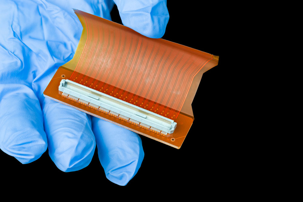
(flex circuit)
- Later, route the individual traces after lacing the drill holes and components like passive components. Then, include markings, labels, and identifiers, in the board layout to show where particular components are on the board.
- Last but not least, generate your layout/design files when the board outline is complete.
- You’re officially ready for PCB assembly, manufacturing, and fabrication (from concept to production).
Best Free PCB Design Software
This section lists legitimate and free circuit board design software/tools for hobbyists.
They are as follows;
- DipTrace is designed software with an easy-to-use feature that does not compromise functionality. It’s ideal for all levels of learning and can operate in systems like Linux, Mac, and Windows.
- EasyEDA: Besides being free, EasyEDA provides a team collaborator, project management tool, library designer, PCB editor, and powerful schematic capture. It also has unrestricted functionality (offline and online) and can work on Linux, Mac, and Windows OS.
- CircuitMaker enables you to design with no restrictions on the PCB dimensions and up to 16 plane layers + 16 signals. It can also help with design rules checking, native 3D visualization, and advanced routing. However, it only works on Windows.
- Autodesk Eagle: The design tool has a PCB layout editor for designing PCBs and a schematic editor for designing circuit diagrams. It is available on Mac, Linux, and Windows and has features like comprehensive library content, PCB routing, component placement, etc.
- Osmond PCB is the only MAC-based EDA design software that supports PCB layout design and schematic capture. Furthermore, it can design boards with up to 700 pins, multiple layers, and unlimited board sizes.
- Fritzing is an ideal PCB design tool for several educational resources because it supports simple circuits, and the software can translate designs onto PCBs, soldered stripboards, or solderless breadboards.
- KiCad: KiCad is a popular open-source design program that links with FreeCAD for physical design, supports GitHub for version control, and integrates with circuit simulation (Ngspice). Despite having a somewhat old-fashioned library structure, it has a powerful suite of functionality and features for experts and beginners.
- Easily Applicable Graphical Layout Editor (EAGLE) is an EDA design program offering designers comprehensive library content, PCB routing, component placement, and more. It can also save Sieb & Myer and Excellon drill files, plus PostScript and Gerber layout files.
Conclusion
To summarize, we may have outlined some rules on PCB design and provided a list of software tools. However, we could have overlooked some design challenges.
Therefore, if you need help, contact us today, and we’ll link you with an engineering expert from our team for assistance.


