Contents
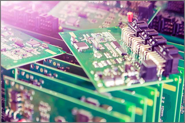
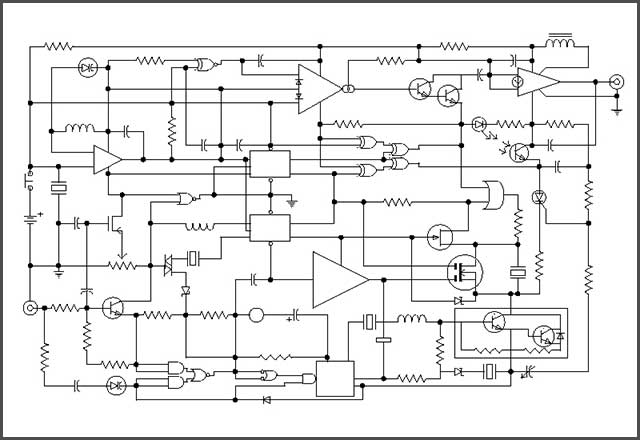
- 1 Printed circuit boards (PCBs) are the brain of almost every mechanical and electronic device. Acting as the center of command, printed circuit boards are essential parts of equipment and electronic circuits. A lack of a sound and well-founded PCB layout or design means that any device it powers may not function as desired. The purpose of this article is to educate you regarding the nine most essential things to note in PCB manufacturing so that you avoid some of the dreadful costs associated with missing the mark. Here they are:
- 2 Design of PCB Stack-up
- 3 Copper Trace
- 4 Via Type
- 5 PCB Manufacturing–Design Documentation
- 6 PCB Manufacturing–The setting of the Direction
- 7 PCB Manufacturing–Signal Integrity and RF Issues
- 8 PCB Manufacturing–Thermal Issues
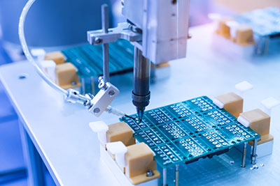
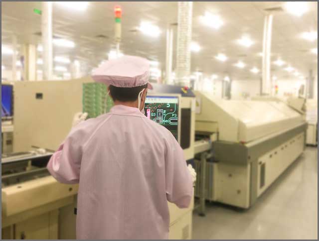
- 9 PCB Manufacturing–The Importance of Testing
- 10 PCB Manufacturing– PCB Layout Issues
- 11 Summary
Printed circuit boards (PCBs) are the brain of almost every mechanical and electronic device. Acting as the center of command, printed circuit boards are essential parts of equipment and electronic circuits. A lack of a sound and well-founded PCB layout or design means that any device it powers may not function as desired. The purpose of this article is to educate you regarding the nine most essential things to note in PCB manufacturing so that you avoid some of the dreadful costs associated with missing the mark. Here they are:
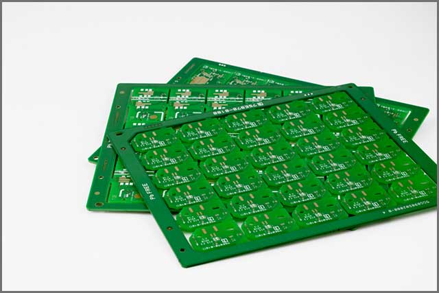
Design of PCB Stack-up
PCB stack-up is the substrate upon which you assemble the entire design components of a printed circuit board. A poorly designed printed circuit board stack-up that consists of inappropriately selected pieces of materials can degrade some essential things such as power delivery, signal transmission, manufacturability, and long-term reliability of the final finished product. If you are in the market for printed circuit boards that will function without failure, you need to work with professionals. You need to work with a company that can design your desired PCB stack-up design up to the number of layers you want using the right materials.
Copper Trace
When it comes to printed circuit board manufacturing, copper is the standard material used in making traces. A PCB consists of several layers, including a solder mask, the substrate, silkscreen, and marks. The trails make up some of the most crucial elements since they carry electrical signals to several different components across the PCB. Without the traces in place, a printed circuit board won’t function as desired.
When designing a printed circuit board, one of the essential elements used in making traces is copper? As a designer, you need to make copper your first choice when making traces. But why choose copper first? The number one advantage of using copper is that it’s highly conductive, meaning that it can easily transmit signals without losing electricity while doing so. Additionally, small tons of copper will do the job, meaning that manufacturers don’t have to use a lot of it.
Via Type
When it comes to circuit board manufacturing, the via that you choose matters a lot; Vias are used to thermally and electronically join pads, traces, and polygons on different layers of a printed circuit board. They are copper cylinders formed or placed in holes that get drilled on a printed circuit board—the type of via that a manufacturer chooses to use matters a lot.
There are three basic types of vias that include blind vias, buried vias, and through vias. Blind vias connect an interior layer to an exterior layer, while buried vias act by connecting two internal layers. Lastly, through vias, connect two outer layers. The type of via to use will depend on the sheets that your board needs. For simple two-layer boards, you may need to use a through via, but for boards with more than two layers, as a manufacturer, you may have to use blind or buried vias in your design, though at increased costs.
PCB Manufacturing–Design Documentation
Plenty of printed circuit board manufacturers, even China correct PCB service provider. Thankfully, there are various PCB manufacturing firms, find documenting their entire design process to be tedious. These manufacturers find this process to be somewhat inconvenient at times. However, design documentation is an essential process that ends up being one of the most critical steps in coming up with a great product.
The printed circuit board design is no exception, and designers have to ensure that they document the right information in the right way. This way, they can manufacture a product that will successfully function as desired. Some of the most vital things that need documentation for successful manufacturing include the bill of materials, manufacturing data, electronic schematics, and other identifying characteristics.


PCB Manufacturing–The setting of the Direction
As a manufacturer, it is essential to ensure that you can orient all similar components in the same direction, especially in evenly arranged columns and rows. Doing this makes it easy to install, inspect, and test all the placed parts with a lot of ease. The direction setting is critical, especially if you are dealing with SMDs or Surface Mount components. For instance, by placing us in the same direction, they’ll be no mistakes made, especially when it comes to soldering and inspecting the board. There’s nothing more frustrating than having to assemble a board with all the ICs facing the wrong direction. Whenever possible, ensure that you keep polarized components pointed in the same direction.
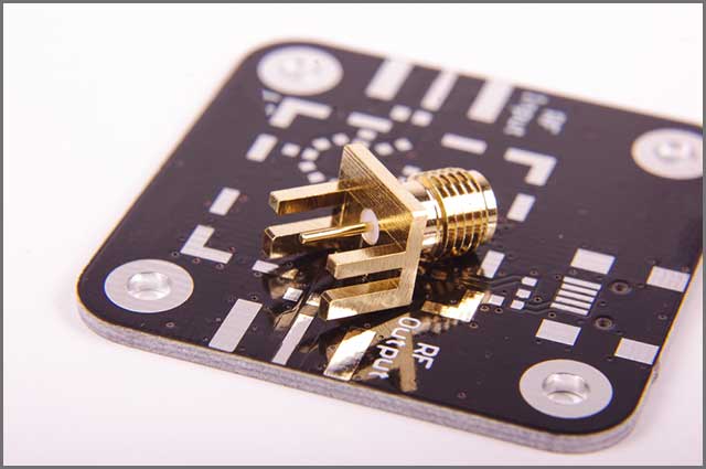
PCB Manufacturing–Signal Integrity and RF Issues
One of the most fundamental challenges associated with high-speed PCB board manufacturing is signal integrity. For a long, loss of signal integrity with printed circuit board units has been an ongoing concern with most PCB manufacturers. Therefore, it is essential to keep in mind matters to do with signal integrity, especially when manufacturing printed circuit boards.
In addition to other transmission issues, to minimize the potential problems related to signal integrity, it is essential to ensure that a PCB supplier of your choice provides printed circuit boards with durable designs. Besides signal integrity, designers of printed circuit boards or RF need to select or use laminate materials that are appropriate for the project at hand. The basis of your choice should meet the electrical needs of the RF circuit, such as loss rate and signal speeds, among others.
PCB Manufacturing–Thermal Issues
With an increasing demand for power-hungry devices lately, trying to avoid your product’s thermal problems is becoming as vital as it has ever been before. Problems could arise in three different areas, namely in thermal relief (the path of heat dissipation during printed circuit board assembly), solder parts (the temperature at the solder joint of your component), and thermal stress (repeated heating or excessive heat). Fortunately, there are specific printed circuit board thermal design actions that one can use to mitigate or handle these potential areas of problem. With the right thermal management techniques or practices, you’ll keep yourself and your board fresh as you go ahead in designing the next revolutionary products.
PCB Manufacturing–The Importance of Testing
Printed circuit boards find substantial use in several electronic components and technologies, an aspect that makes them some of the most valuable devices. Whether it’s a mobile device, computer, or any other sophisticated machinery, printed circuit boards are responsible for how the device functions. If some defects while manufacturing them, they can bring about malfunctions with the final product and bring about inconveniences. Even when it comes to electronic contract manufacturing, manufacturers may have to recall their devices and spend additional time and other resources towards fixing the malfunctions.
This is one reason why a majority of printed circuit board developers turn to PCB designers and manufacturers for testing. Testing is one of the most critical stages in the manufacturing process of PCBs. Without trial, PCBs may reach the final consumers with errors and problems ignored during the production phase. But to minimize the chance of failure while maintaining customer satisfaction, it is essential to ensure the implementation of testing procedures. This way, manufacturers will ensure that the PCB and its entire components function as desired.
PCB Manufacturing– PCB Layout Issues
Printed circuit boards are essential components of a majority of electrical devices that we commonly use today. However, when it comes to customs electronics PCB layout issues during the manufacturing process, such as over-etching or drilling errors, which can be catastrophic. Other PCB layout issues include plating voids, insufficient copper-to-edge clearance, missing solder masks between the pads, and starved thermals. Luckily enough, we at WellPCB are all aware of PCB layout issues, why they occur, and how we can help you avoid them.
Summary
Printed circuit boards are essential components that power a majority of electronic components and plenty of other equipment that we use today. However, when it comes to the manufacture of printed circuit boards, there are some essential considerations that manufacturers need to be aware of at all times. We at WellPCB have highlighted for you 9 of the essential points to note regarding the manufacture of printed circuit boards. With the above, rest assured of coming with a board that functions as desired.


