PCB Manufacturing Defects and Solutions Being at the receiving end of a printed circuit board failure can be annoying and dissatisfying. Thus, these defects lead to a higher risk of time, products, reputation, and money wastage.
Understanding some of the common defects can help you perform some analysis and proffer solutions to ensure the quality and sustainability of cheap PCB. Therefore, we have compiled a list of some of the common PCB failures. They include;
Contents
- 1 Pin and Connector Checks
- 2 Heat Dissipation Analysis
- 3 Chemical Fluid Leakage
- 4 Solder Bridging (Shorts)
- 5 PCB Manufacturing Defects and Solutions–Missing Components (Component Shift)
- 6 PCB Manufacturing Defects and Solutions–Wire Breaks
- 7 PCB Manufacturing Defects and Solutions– Open Solder Joints
- 8 Conclusion
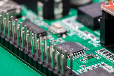
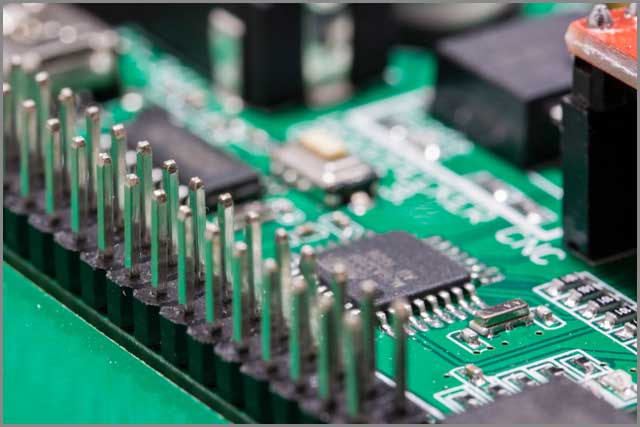
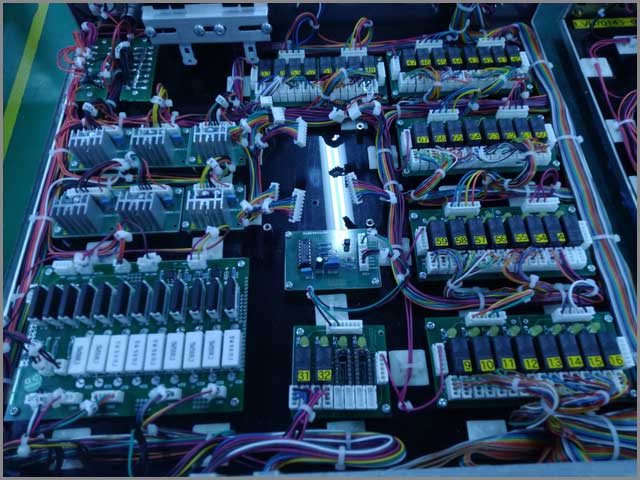
Pin and Connector Checks
One of the important components of PCB is the pin and connector, which help relay signals in operations. Incorrect placement of the pin can result in damage to the connector. To prevent this defect, you can use a pattern-matching tool to check the connector’s correct placement.
Thus, you can use this pattern-matching tool, usually in a vision tool kit, to locate and group patterns. Hence, it provides a score that indicates how much the patterns match the intended pattern or location.
However, to ensure the alignment of pins, you can use a telecentric lens. The magnification of a telecentric lens does not change, which prevents parallax error, which a conventional lens can cause.
However, a thorough check of pins and connectors will go a long way in preventing this defect in cheap correct PCB service provider. Thankfully, there are various PCB manufacturing companies.
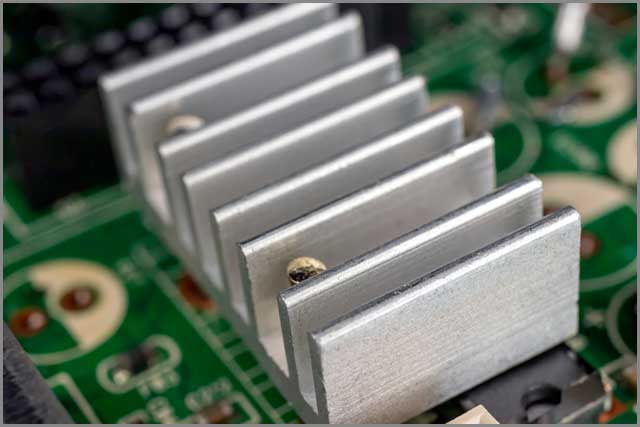
Heat Dissipation Analysis
Most electronic components tend to get unusually hot whenever they are working at their full capacity. Hence, this can lead to overheating if they are not properly checked. Also, a hot PCB heat sink can be a shock to unsuspecting technicians.
Likewise, PCB’s extreme temperatures can lead to a reduced lifespan of products hence. Leading to a waste of money and the poor reputation of manufacturing companies.
Thus, to protect your PCB design from overheating. You will have to solder an SMD heat sink, which usually has a thermal pad against a heat spreading pattern on the PCB. Also, an SMD heat sink is then soldered on the end of the copper, which will promote better dissipation of heat.
Furthermore, you must ensure that the safety limit is not exceeded. The heat sink is not overly hot, such that it can damage the skin.
By using an SMD heat sink, however, heat will dissipate in proper measures in high power components. Thus, ensure that you use the SMD heat sink’s right size or shape when soldering it onto the PCB.
Chemical Fluid Leakage
The case of PCB failures is no longer news. Typically, as an assembler, you will have come across a PCB failure before. Thus, it is vital to carry out failure analysis tests that you will use in identifying and solving the problem at such times.
The leakage of chemical fluid can generally lead to severe damage of the printed circuit boards. However, this leakage can be due to leftover trace elements that were not properly removed during the PCB manufacturing process.
Also, a chemical fluid leakage can occur inside the packaging of a component, which can pose a risk to the component, thereby damaging it or making it corrosive.
To prevent chemical leakage, manufacturers should ensure thorough cleaning of circuit boards to avoid chemical residues, causing corrosion of the boards’ metallic parts.
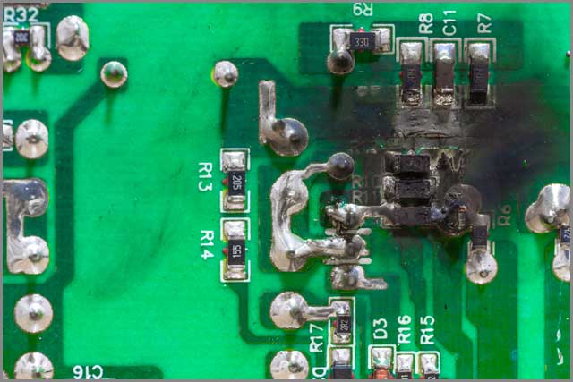
Solder Bridging (Shorts)
Over the years, solder shorts have been a common occurrence in the wave soldering process. Solder bridging occurs due to the inability of the solder to separate from two or more leads before the solidification of the solder. However, it is often not easily noticeable, making the havoc it wreaks on the component less desirable.
Various factors can cause solder shorts during the production and manufacturing of PCB. These factors include the number of pins and proximity, poor fluxing, excess paste, poor solderability of the pins, the reflow oven setting, and wave separation, amongst others. An increase in the contents on boards generally leads to short problems.
Thus, to reduce solder shorts, you can employ the use of good design rules, lower component lead length, and reduce pad size. Also, a careful stencil modification can control the dispensation of the solder paste on the pad, which can lead to a drastic improvement, which leads to solder bridging avoidance.

PCB Manufacturing Defects and Solutions–Missing Components (Component Shift)
The component shift means the misalignment of a component to its target. It is a common occurrence during reflow due to the ability of the components to move/flow on the molten solder.
In other words, some components may misalign themselves as a result of the tension on the surface of the molten solder. Some of the major factors that cause component shift include an excessive increase in the convection rate, bent leads, rapid vibration in the conveyor systems, wrong placement of solder, and lopsided component heat sinks.
Thus, to prevent a component shift in the manufacturing of PCB, it is advisable to maintain the correct temperature and humidity levels, decrease the number of movement in un-reflowed assembly and increase the solderability of PCBs by using a tough flux.
PCB Manufacturing Defects and Solutions–Wire Breaks
In general, detecting a wire break on a PCB can pose a problem to manufacturers. Even though it is simple to tell when there is a wire break on the board, pinpointing the break’s location is the major problem.
Wire breaks can cause a PCB not to work, and thorough inspection can save the product from becoming useless.
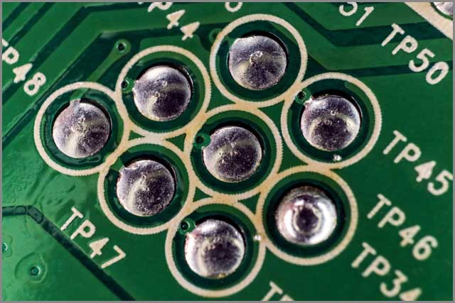
PCB Manufacturing Defects and Solutions– Open Solder Joints
One of the major causes of open solder joints is a separation between the component lead and the PCB pad. It can also result from the failure of soldering the PCB pads to the component lead due to lack of solder paste or the inconsistency of solder paste deposits.
Thus, to avoid open solder joints, ensure the right PCB design and correct placement. Also, avoid the contamination of solder paste due to exposure to the environment and correct the aspect ratio.
By correcting the aspect ratio, which is the ratio of the aperture width to the stencil thickness, open solder joints can be effectively fixed.
Four layers PCB is a form of multilayer PCB, consisting of four layers of copper, which you can laminate together and hold by resin layers. You can use it in various fields, including telecommunication and vehicle manufacturing. In recent years, buyers want faster and high-performance electronics, which has made the demand for multilayer PCB to rise.
Thus, PCB production requires specialized equipment and expertise and the manufacturing of proper functioning electronics for the benefit of buyers and electronic enthusiasts.
Conclusion
There you have it, the seven most common cheap PCB manufacturing defects and solutions. As earlier stated. It takes proper analysis to detect these faults. Improper and delayed detection can lead to the latent failure of PCB, and it can threaten manufacturing companies’ success.
Want to Contact an expert today. At WellPCB, we offer lasting solutions to PCB failures and provide helpful analysis that can help transform PCBs’ faults and defects and prevent future failures.
Visit www.wellpcb.com for more information.


