Contents
1. What Is Wave Soldering?
Before deepening the definition, let’s look at the various types.
There are five major types of wave soldering:
1. Manual
2. Drag
3. Selective
4. Dip
5. Wave
Manual soldering isn’t found in every production space nowadays. Although some engineers still actively use this method.
It requires highly experienced labor. However, the number of boards created by these experts is limited.
Drag and Dip was introduced many years ago as a more affordable alternative.
However, they have become outdated today. Hence, newer and more affordable wave systems have emerged.
So, now to the definition. What exactly is wave soldering?
It’s straightforward. Wave soldering is a PCB production process that consists of bulk soldering. So, it involves a PCB passing over a pan of molten solder.
By doing so, the pump creates an upwelling of solder that resembles a standing wave.
So, components get soldered to the board. And it happens when the circuit board connects with the wave.
In the last stage of the wave soldering process, something happens. The components become glued to the PCB surface via placement equipment.
Then, it runs through the molten solder wave.
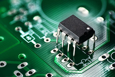
Also, wave soldering is ideal for soldering through-hole components. Nowadays, surface-mount PCBs have replaced through-hole PCBs.
But this applies mainly to small-scale electronics. In such cases, engineers use reflow soldering applications.
Nonetheless, surface-mount PCBs aren’t suitable for large-scale devices. That’s why simple through-hole PCBs outshines.
2. Wave Soldering Process/ What Are the Five Steps of Soldering?

Wave soldering is an in-line process that treats a PCB with flux. Afterward, it preheats and immerses the PCB in liquid solder.
Thus, you should know that various solder machines are available, and they all vary in their processing.
However, the devices have similar principles and components. For instance, a primary part used is a conveyor. Hence, this conveyor moves a PCB via various zones.
But that’s not all.
There are four other necessary components found in every solder machine.
1. There’s a flux sprayer.
2. It has a preheating pad.
3. The device has a pump that creates the actual wave.
4. It has a pan solder.
Also, solder is a combination of metals. Hence, the leaded solder has various chemical mixtures. It contains 0.5% antimony, 49.5% lead, and 50% tin.
So, here is the step-by-step process of wave soldering:
Step 1: Melting the Solder
Melting the solder is the first step. Hence, it’s the most key process. The wave soldering machine has a tank containing solder.
To kickstart this process, you must heat the solder. By doing so, you’ll melt it to its purest form. Afterward, you must ensure that the solder reaches the right temperature.
That way, the process will be more consistent. This makes the wave soldering process smoother.
Step 2: Dusting the Components
This step is another very essential one. Before soldering components, you should clean through. So, while cleaning, check to confirm if there are any oxide layers.
If there are any, you need to clean them. It would also help if you prevented them from forming oxide layers.
Experienced engineers know the process as fluxing. Furthermore, there are two major types of fluxing.
Step 3: PCB Placement
After carrying out the above steps, the next is to consider the PCB placement. That’s when you place your PCB in the melted solder.
But that’s not all.
The PCB gets support from the metal clasps of the solder machine. By doing so, the board maintains the placement and firm positioning of the PCB.
Step 4: Solder Application
Now that you’ve correctly placed the PCB, you need to consider the solder application. You must ensure the solder settles entirely within the joints.
Plus, it would help if you did everything to avoid bumps from forming.
Step 5: Cleaning
In wave soldering, cleaning is the last stage to consider. Nevertheless, it’s still as essential as the first step. By cleaning, you’d have to dust the flux residues. So, you can clean and wash the circuit boards with solvents and deionized water.
3. Wave Soldering Machine
A wave soldering machine comprises a heated solder tank. And it gets maintained at a specific temperature for the soldering procedure.
But that’s not all.
A solder wave is usually inside the tank. And the PCBs pass over the board’s underside. So, at that point, the board connects with the solder wave.
Also, you must tread with caution when adjusting the wave’s height. By doing so, you’d be keeping the wave from flowing over the board’s anterior side.
It’s at this point the solder gets to the required places.
Also, the PCB holds up tight in a segment on the conveyor thanks to the metal fingers, which can withstand various temperatures.
The reason is that its material is titanium in nature. Plus, the solder doesn’t affect it.
Preparation with a Solder Wave Machine
An electronics PCB needs something to be successful with a solder wave machine. It requires perfect design and production.
So, here are two standard precautionary methods for solder wave machines.
Solid Resist Layer: This preventive method is the standard practice for designing PCBs nowadays. It involves adding a layer of varnish material to the PCB.
However, the solder hardly adheres to the PCB, so only the areas that require soldering are left open. Plus, most of the solder resist is green.
Pad Spacing: This second precautionary method is also essential. It helps to ensure enough spacing between pads that require soldering.
It’s detrimental for the pads to be too close. Plus, bridging may occur if two pads are too close, leading to a short circuit.
4. Wave Soldering vs. Reflow Soldering
A lot of people find it difficult to identify something. And it’s differentiating between wave and reflow soldering. The reason is that many engineers don’t know their differences. Also, that’s why we chose to illustrate their differences here clearly:
4.1 Soldering Process
The wave soldering process usually contains flux spraying. But reflow soldering doesn’t entail flux spraying.
4.2 Soldering Reliability
Instead, it’s best to get expert assemblers who comply with the production policies. That way, you’ll avoid unforeseen defects.
4.3 Selection Standard
Typically, reflow soldering is ideal for surface mount technology. And wave soldering is perfect for DIP or through-hole technology. However, it hardly happens that a PCB only contains THT or SMT components. What usually happens is that fabricators use SMT devices that can withstand higher temperatures than THT devices.

5. Selective vs. Wave Soldering
If you deal with PCBs, you should be familiar with selective and wave soldering. After all, they are standard PCB soldering methods.
But, each method comes with its merits and demerits. Afterward, that’s what separates them. So, here are things you should know about them before you make a decision:
What Makes Wave Soldering Unique?
It’s a process that occurs in a protective gas atmosphere because nitrogen is present. Plus, nitrogen helps to avoid solder defects to some extent.
The wave soldering method is quite useful for volume production. However, it has some drawbacks. First, its operating costs are high.
Also, it consumes a high amount of flux. And it consumes a lot of electricity.
What Makes Selective Soldering Different from Wave Soldering?
It’s a useful method for soldering PCBs. It’s a type of wave soldering, and this method applies specifically to PCBs assembled with through-hole parts.
It’s unsurprising that this method is gaining popularity. Double-sided PCBs are a thing now, permitting lighter and smaller products.
One benefit of this method is the reliability of the solder joints. It also permits setting different parameters for each part.
Plus, the process doesn’t need an expensive aperture wave solder part.
Selective soldering also has some snags. First, you may experience processing errors, and that’s because it has a host of parameters.
Plus, the procedure is time-consuming. And it’s because each circuit board needs a unique program.
In summary, both methods are ideal.
However selective soldering works best for a simple board that allows consideration of some parameters.
Wave soldering is also the best option for boards with large surface-mount parts and through-hole components, as well as for mass production.
Selective Wave Soldering Guidelines
Before using the selective wave soldering method, following some rules is crucial.
You can carry out this process in three stages.
Firstly, you have to sort out the parts that need soldering. Then, you can apply liquid flux to the various elements.
Secondly, you have to preheat the board. The day, you can solder specific components with the fountain of solder.
6. Dip Wave Soldering
Dip wave soldering is an automatic process. It’ quite useful for the mass production of electronic products. The method offers product quality and efficiency.
With that said, the method begins with a PCB board. But the board must have gone through some processes like printing, curing, etc.
Afterward, the PCB will move forward alongside the conveyor belt (located at the machine’s inlet end).
After this, the board will pass through a spray tank.
At this stage, the PCB will receive a thin flux layer on its underlying surface and pins. The board plate will then move down to the preheating zone.
In this zone, the flux will lose its solvent. The active agent and resin in the flux will decompose and activate.
During this process, you need to preheat the board and parts thoroughly.
The bottom will experience its first molten solder wave as the board moves forward.
This wave helps print the welding flux on the PCB. Then, the second molten solder wave hits the bottom of the PCB.
This smooth wave helps to divide the connecting bridge between the welding end and the pin and removes welding defects.
7. Wha Are the Factors to Consider for Wave Soldering?
Here are a few factors to consider for wave soldering.
They are as follows:
7.1 What Is a Wave Solder Pallet?
A wave solder pallet is an insulating material that helps to streamline the circuit assembly process. It also eliminates the need for manual labor and human resources.
7.2 Wave Soldering Temperature
Regarding wave soldering, the temperature should be between 180 to 2250C.
7.3 Lead-Free Wave Soldering
Before you convert to lead-free soldering, it’s crucial to consider a few things. First off, you should consider the wave solder pot.
After all, it’s specifically for lead-free soldering. Plus, it contains lightweight titanium hardware and higher-grade stainless steel parts.
What if you’re dealing with Sn-Ag-Cu alloys?
In this case, you have to either get a new solder pot. Or ou can opt for a new wave solder machine. And it’s because Sn-Ag-Cu alloys react aggressively with the materials in most older wave solder machines.
Can I work with an existing wave solder equipment?
If you insist on working with old wave solder equipment, you should know one thing: It needs more maintenance than newer equipment.
7.4 Wave Soldering Defects
No doubt, there’s a higher level of accuracy with wave soldering compared to manual welding.
Plus, the process has a lower error rate.
But, it’s crucial to control the welding content and position. Otherwise, you may easily experience the following defects:
1. Los film
If the curing temperature is extreme (too high or low) or the quality of your adhesive is poor, you may experience a loss of film.
2. A d formed PCB
3. Dir y board surface
A dirty PCB surface often occurs with extreme preheating temperature or a highly reliable flux content.
4. old solder
A cold solder happens when the welding temperature is extreme.
Or there’s the oxidation of the pins or pads. It also occurs when the conveyor belt’s mechanical vibration disturbs the solder joints as they cool.
5. lu residues
6. ol r ball
If your substrate construction is low, you may have a solder ball. This can also result when the PCB is wet during storage or has high ambient humidity.
7. sh t circuit or Solder joint bridge
A short circuit may be caused by low solder resist activity or by narrow pad spacing in your PCB design.
8. om tones
Tombstones occur when you use parts with different temperatures or solder-type requirements.
9. na quate hole fill
This defect may happen if the solder resists flowing into the holes and has poor quality. r the solder viscosity is low due to extreme PCB preheating.
10. ow setting
This defect occurs when a solder doesn’t spread well on a pad. Hen this happens, you won’t get a good solder. His directly affects the reliability of the solder joint.
FAQS:
What are the disadvantages of wave soldering?
One of the biggest disadvantages of wave soldering is high solder, flux, power, and nitrogen consumption.
These requirements can make wave soldering more costly than other techniques.
Additionally, wave soldering requires you to carefully mask and cover the sensitive areas of the PCB before actual soldering can commence.
This process can be tedious, but it isn’t the only time-consuming aspect of wave soldering.
Post-wave-soldering operations, such as solder reworking and cleaning of soldered assemblies, apertures, and equipment, can add time overhead.
What is the difference between manual soldering and wave soldering?
Wave soldering is a (mostly) automated process where fabricators pass multiple printed circuit boards through a bath or stream of hot molten solder.
Manual soldering involves soldering circuit boards by hand. The skilled technician usually performs manual soldering.
Manual soldering is suited for small and specialized productions, whereas wave soldering is intended for bulk orders.
What flux is used for wave soldering?
Fabricators use a flux that is either free from or has low volatile organic compounds (VOC) for wave soldering. The wave soldering flux must also have a low solids content (<= 2%).
What are the advantages of wave soldering?
Wave soldering makes mass production of PCBs easier. Additionally, it’s currently the only effective way to solder through-hole components. Av soldering also allows for cost scaling and is far more cost-effective than manual soldering or reflow.
In Conclusion
There you have it—a comprehensive breakdown of wave soldering. Now, it’s up to you to cherry-pick the wave soldering process that works best for you.
While at it, it’s essential to consider factors like the board components (surface mount or through-hole).
You should also factor in the type of production you plan to execute.
As mentioned above, other factors are its defects, wave soldering temperature, wave solder pallets, and lead-free wave soldering.
P.S:
What do you think about this piece?
Please get in touch with us if you have any personal suggestions or worries about this topic.