Contents
- 1 Sprint Layout
- 2 Sprint Layout 6.0
- 2.1 Bigger Resolution And Accuracy:
- 2.2 Pick+Place Data:
- 2.3 Anti-Alias:
- 2.4 Multi-Select:
- 2.5 Selector:
- 2.6 Automatic Capture Mode:
- 2.7 Gerber Import:
- 2.8 Rubber-Band:
- 2.9 Components:
- 2.10 1Thermal-Pad Vias:
- 2.11 Isolation Milling:
- 2.12 Grid-Hotkeys:
- 2.13 Rectangle:
- 2.14 Circular Arrangement:
- 2.15 New Crosshair:
- 2.16 Sprint-Layout Full Crack
- 2.17 Sprint-Layout Export
- 3 Sprint Layout Tutorial
- 4 Sprint-Layout Usernote
- 5 Conclusion
Sprint Layout
Sprint layout had several tools to draw things like tracks, solder pads, zones, text labels, SMD pads, and many more; it comes along with all necessary functions for board design.
Even professional features like the export of Gerber-files (which are supported by almost every PCB manufacturer. If you own a CNC milling machine) or isolation-milling that have HPGL created for them are included.
The software construction of sprint layout is made self-explanatory; with the free viewer-software for Sprint-Layout, everybody can view or print your designs.
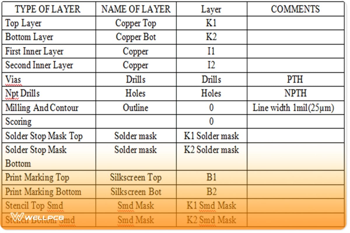
Two layers exist (Copper and silkscreen) for each side of the board. You have the option to use an outline layer for the board contour or two additional inner layers for multilayer boards. Extra features are solder masks, SMD masks, automatic ground planes, signal flow tests.
The Photoview option gives you a chance to take a look at your board as if it was manufactured.
This option helps you to find faults on your board. Several components for through-hole or SMD layouts have been predefined in the extensible library.
Many options are selectable when printing the design, the component mounting plan, or the solder mask on paper or film. The software also has an extensive and comfortable printing option that allows you to print your layouts or component mounting plans on paper or foil.
You can export your layout to a BMP, GIF, or JPG format. These other formats can be used in document programs like Word or on your homepage for publishing.
There is an auto-router to connect individual tracks integrated into the software, but we warned that sprint layout is not made for automatically routing complete boards. The sprint layout will create Gerber and Excellon files for the professional manufacturing of your board.
Sprint Layout 6.0
The Sprint layout 6.0 is one of the latest versions, and like with every new release, you get new features. New features you should take special notices of include:
Bigger Resolution And Accuracy:
Unless other previous versions, you increase the resolution and the accuracy of the sprint layout by tenfold. You should know this concerns the Grid settings and the maximum zoom factor. So there is no problem designing incredible layout structures.
Pick+Place Data:
The sprint layout can now generate and export pick+place files. You need these files for automated assemblies of SMD boards.
Anti-Alias:
The use of the anti-alias technology to noticeably improve the graphic representation of the sprint layout has been applied in the new software.
Multi-Select:
Simultaneous editing of several elements: you can now edit as many items as you want simultaneously with the properties panel.
Selector:
The new version of the selector is now a more powerful tool; with this tool, you can find and select specific elements of your layout and edit them simultaneously with the help of the new multi-select function. A good example would be picking and cleansing all pads with a specific shape or drilling.
Automatic Capture Mode:
You have a new mode of capture, making pads and tracks easy to place; if the mouse moves closer to the capture point, the mouse’s energy will be captured and helps you to connect precisely. It is beneficial when some connections are lying out of the light.
Gerber Import:
You have the luxury of a Gerber import which allows you to load existing Gerber files and convert them to a ready layout inspiring-layout.
Rubber-Band:
While moving elements, you have connected tracks that can keep their connection.
Components:
6.0 can now display and manage components, including identifier and value. Even a component list is available.
1Thermal-Pad Vias:
You can now define the thermal pad separated for each layer when/if you use vias as a thermal pad.
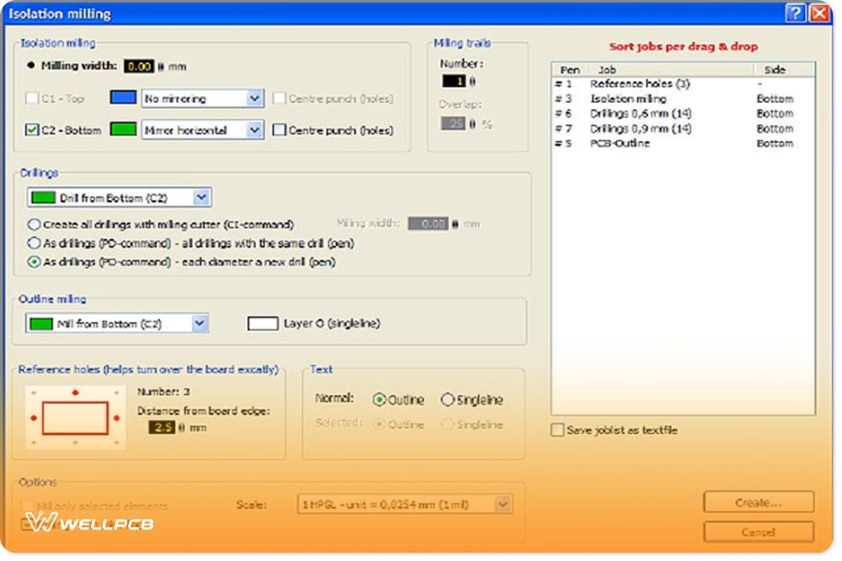
Isolation Milling:
Usually, all individual jobs like isolation milling, drilling, or cut-out had to be done in different plot files, but now the isolation milling has been revamped, all those jobs can now be written in one plot file. So the typical problems with the origin in various files will be prevented.
Grid-Hotkeys:
The key (function essential 1-9) on your keyboard is given specific editable grid values. So you will be able to change between several grid values with just one keystroke.
Rectangle:
You can now draw rectangles (tracks or zones) quickly with the new rectangle drawing mode.
Circular Arrangement:
The specific circular method is a tricky and unfair job. Sprint-layout now has a special assistant for that. Once you define the necessary parameter, you will see the result of your parameters in a preview before you complete the action.
New Crosshair:
You have an improved crosshair, which is consistently involved in every action and can display an additional 45° lines and the numeric values of the coordinates directly on the crossbar.
Sprint-Layout Full Crack
Now I guess you are wondering, what’s the difference besides the obvious that the words “Full crack” indicate. Well, like previously stated, Sprint-Layout is electronic software used by Windows systems.
One of the versions is the sprint-layout full crack for the Windows OS that is easy for everyday use.
This software comes in a clean and neat user interface. It is easy to use and lets you work more efficiently. There are hotkeys that you can use and customize for specific functions.
The software specifications for it to work on a laptop/desktop are below:
System Requirements: Operating System: Windows XP/Vista/7/8/10
Memory (RAM): 1GB of RAM required.
Hard Disk Space: 400MB of free space required.
Processor: Intel Pentium 4 or later
Sprint-Layout Export
You know all about the new features of the sprint layout 6.0, but one of the most important functions is the Export function and its many types/formats of exporting
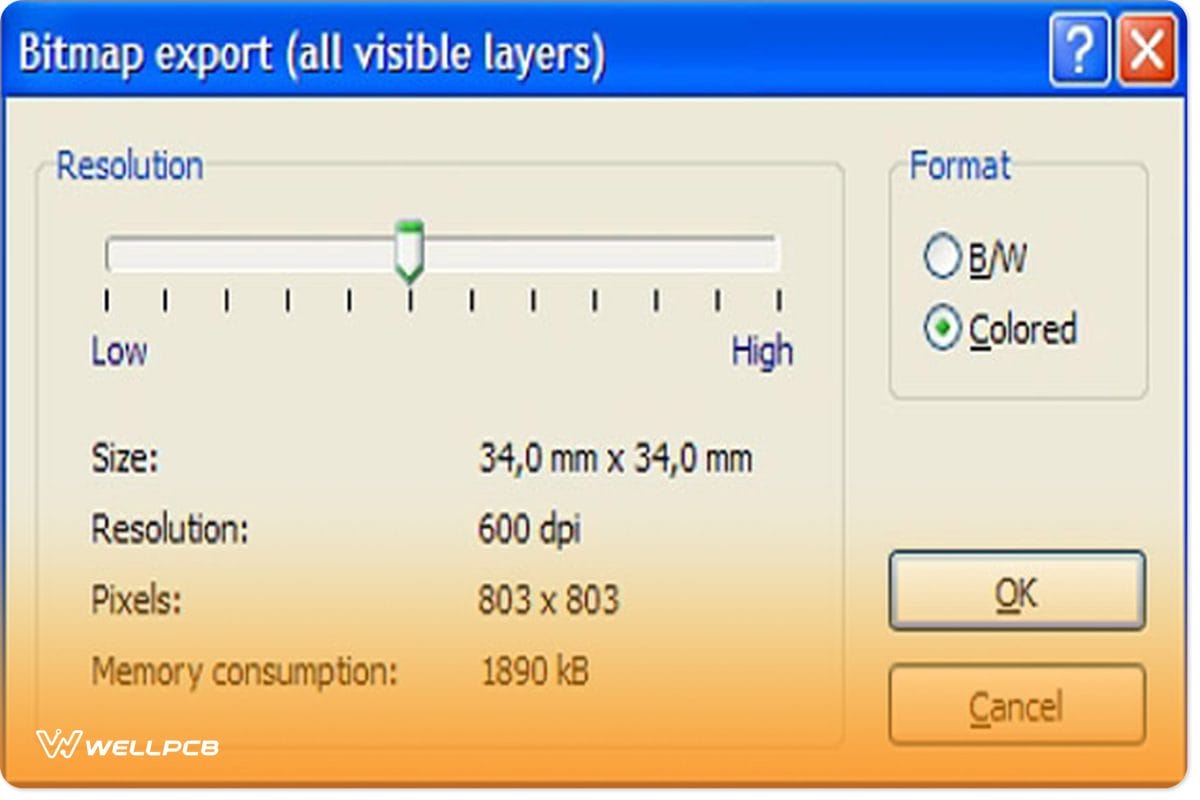
Bitmap-Export:
This function allows you to create a bitmap(.bmp) that may be used with other applications. The layers that are visible in the editor are where the bitmap is created.
GIF-Export:
This allows you to create a GIF file (.gif) that may be used with other applications. The layers visible in the editor are where the bitmap was made from, and the GIF format is a compressed format, so you get a much smaller file than the bitmap.

JPEG-Export:
This allows you to create a JPEG file (.jpg) that may be used with other applications. The layers visible in the editor are where the bitmap is generated from; the JPEG format is a compressed format, so you get a much smaller file than the bitmap.

Gerber-Export:
Gerber files are known to nearly all manufacturers because every layer (solder mask, copper, silkscreen) needs a Gerber file to describe a PCB completely. You can exchange layout data with manufacturers because the Sprint layout produces a standard Gerber-files RS274-X widely used.

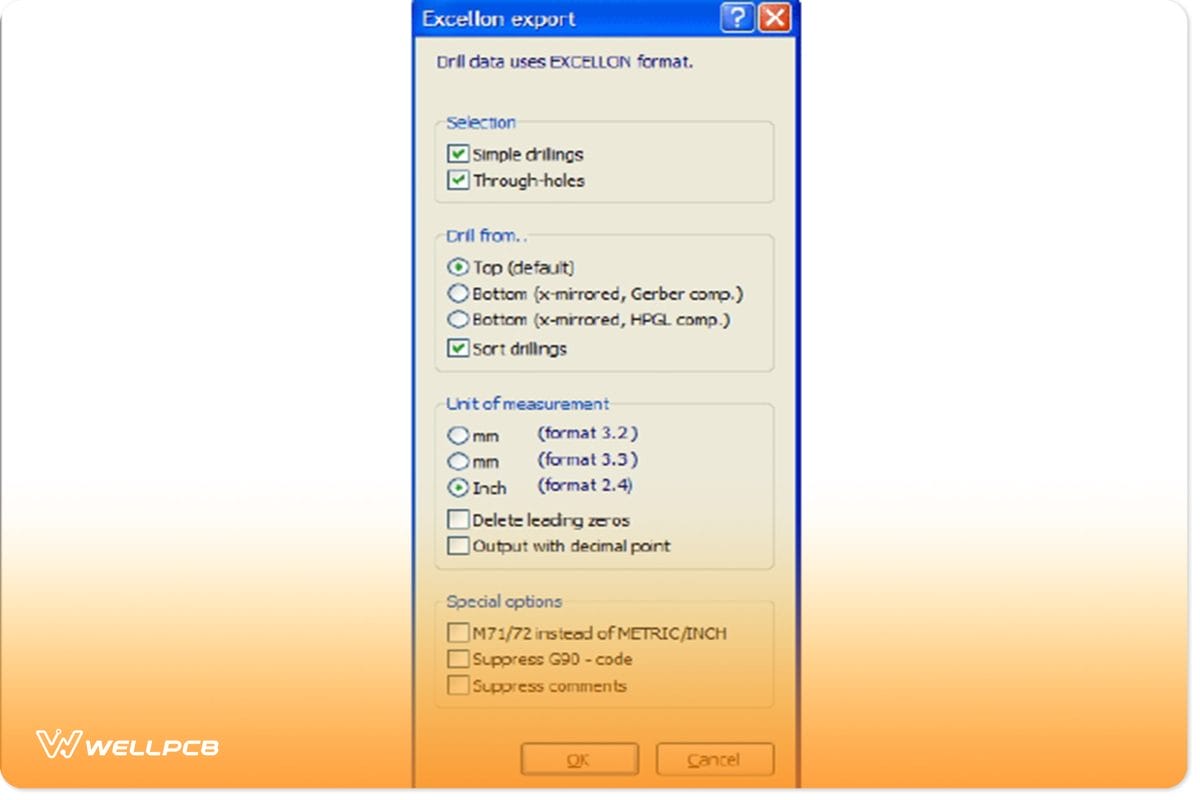
Excellon-Export:
This is used to exchange the drill data of a board with your manufacturer. It contains all diameter and positions of your drilling.
Isolation-Milling:
This is a particular function to produce PCBs with a CNC milling machine. The track and connections will be milled out of the solid copper board. The production of an isolation-milled board, including the isolation channels, the drillings, and the board shape, is all supported by Sprint-layout.
Everything gotten will be exported in a plot file in HPGL format (*.plt). A CNC milling machine will then use this plot file to produce the board.
Sprint Layout Tutorial
If you wish to create your own Circuit board Layout with the ABACOM sprint Layout program, here are a few tutorials and tips: always use all the prescribed standard layers of the sprint layout.
Most manufacturing companies will generate the production data (Extended Gerber) for you if it’s in its current layer.
Another thing is the Gerber Export; if you want to make the Garber export yourself, you can follow these steps:
- 1: Choose layer that will be changed to Garber

- 2: Then press create Gerber files
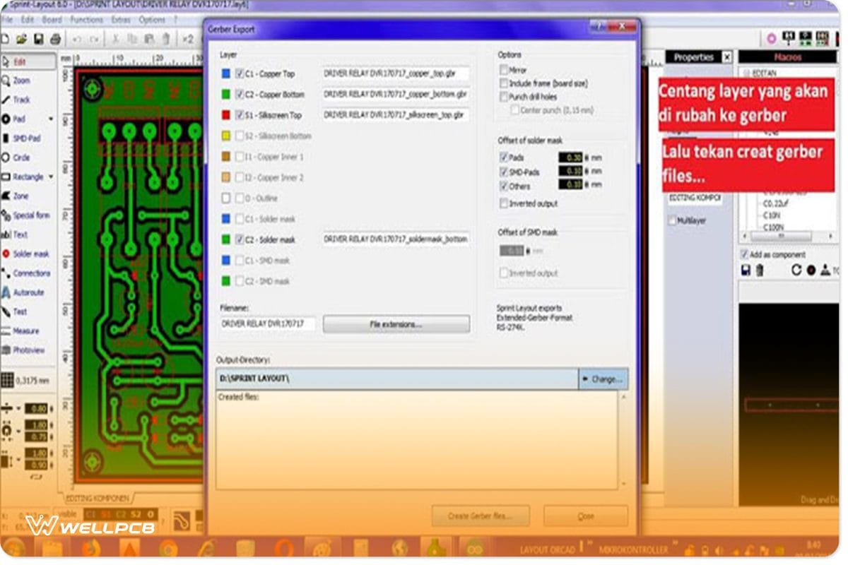
- 3: The file has been successfully changed to Gerber, then press close

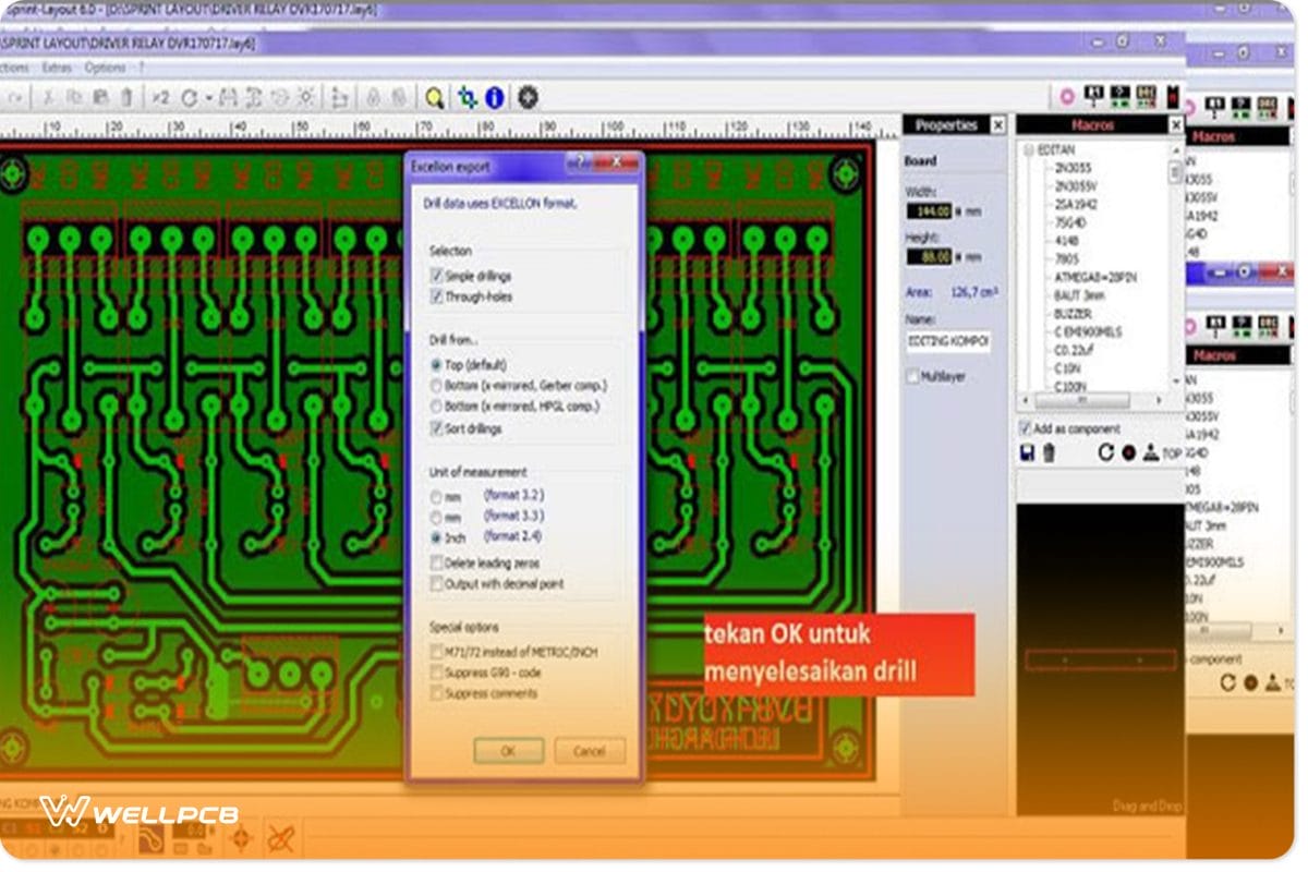
- 4: Press the export drill data file (Excellon). This step is to make the Gerber want to be a hole.
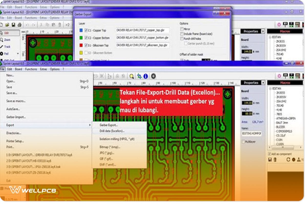
- 5: Press ok to complete the drill
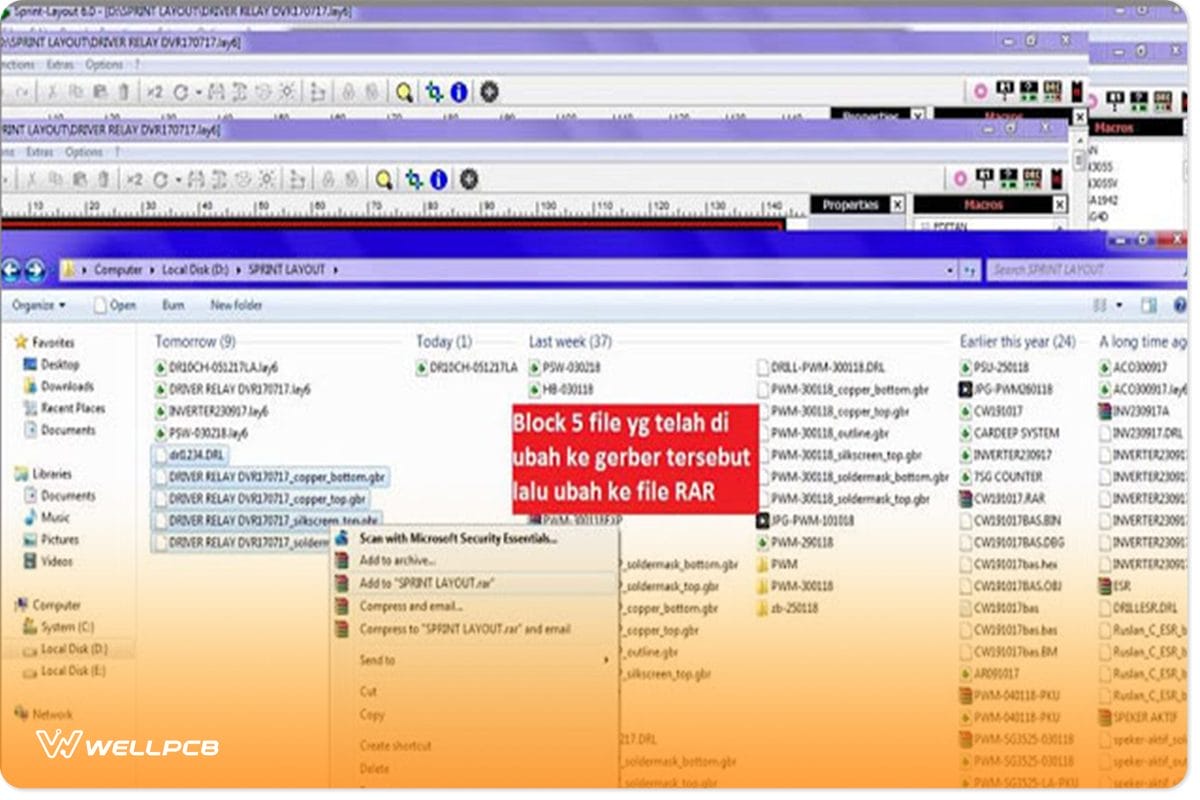
- 6: Collect each layer file and achieve them into a Rar. Format
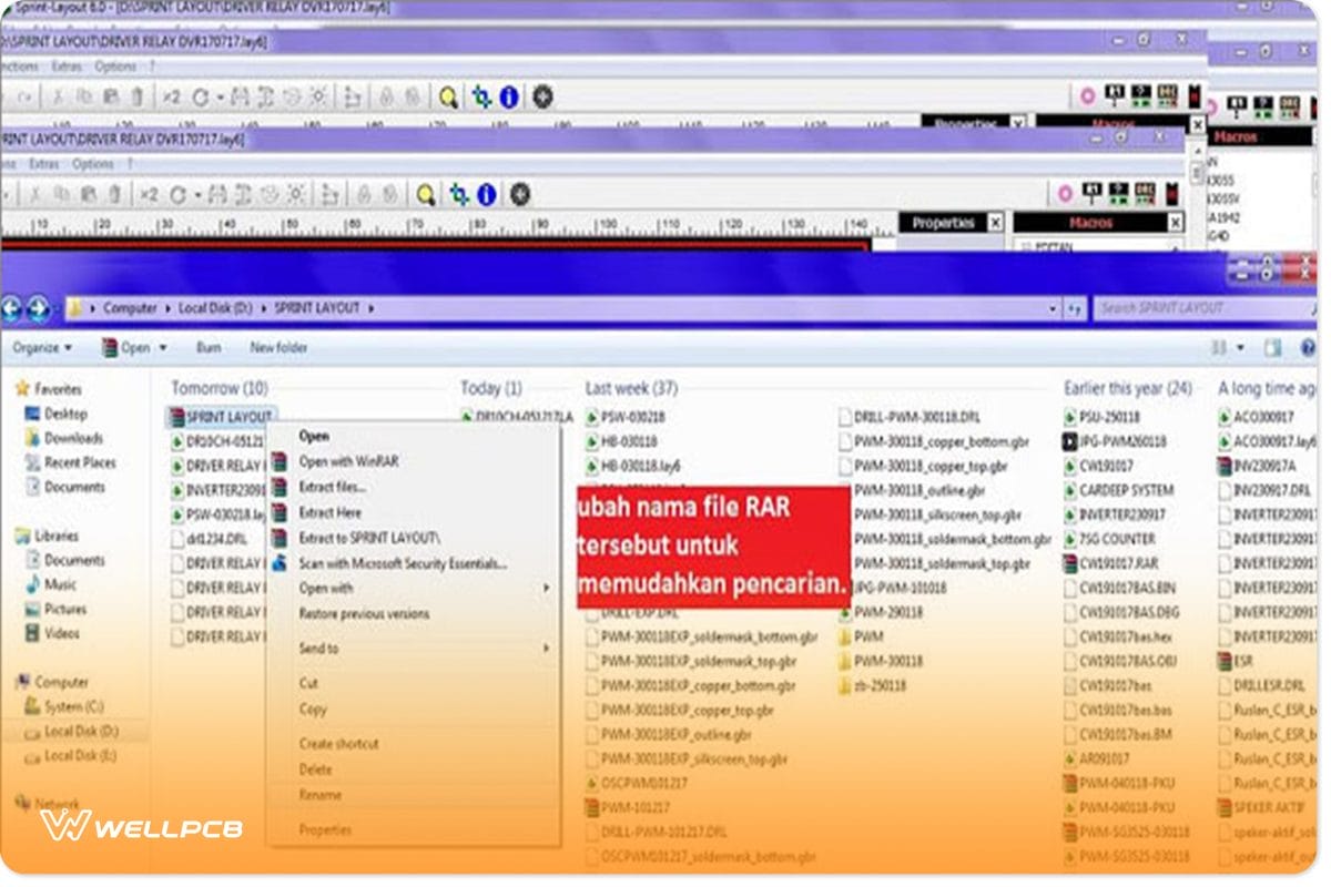
- Step 7: Rename the file and send it to your PCB manufacturer
Among the options, the “Mirror” option should not be chosen in any case, and in regards to the solder mask offset, always make the clearance of the solder mask to 0.5mm (50µm), as this is the least tolerance that a solder pad allows for any solder mask to be applied.
Just remember that the finely pitched components will not have an adequate solder mask bridge between the pads for any more significant value.
However, if you feel uncertainty, you should remember; when in doubt, do nothing or, in this case, leave it at 0.00mm; the manufacturers optimize this.
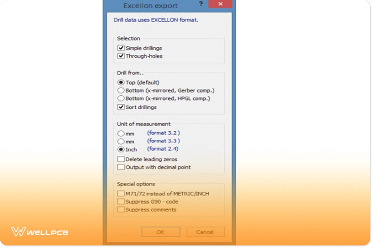
Also, for exporting drilling data, please always choose the unit of measurement to be 2.4 inches.
Sprint-Layout Usernote
PRO
• I saw this program as a very advanced drawing program and advanced with PCB design in mind. The viewer software is much more than a viewer: it allows you to calibrate your printer and print out the PCB design for home manufacturing the PCB. It has Gerber and Excellon support, so also suitable for professional manufacturing.
• I opted for Abacom’s Sprint-Layout. I have not used Eagle, so I can’t truly A-B them, but I have used ExpressPCB software (which I loved, just not their PCB prices).
I found Abacom’s Sprint-Layout very easy, intuitive, their help files return usable information, and it is straightforward to create/modify device footprints. A fully functional PCB CAD software that is reasonably easy to learn and use all while being stable is a bargain
• I’ve also used FreePCB (I have the utmost respect for free, open-source apps, but I would not say I liked it) and the accessible version of DIPTrace (the free, pin-limited version) and still prefer Sprint-Layout.
Also, I received my professional boards yesterday, and they are beautiful and perfect. Now I’m thrilled with Sprint having gone from schematic to completed board so quickly and easily for a bargain software package.
• I chose this program because it’s so simple to use (I am fond of simple things ;), and I also use it for timing diagrams. It allows you to import a scanned copy: handy.
Cons
• Abacom also has a Schematic Editor, sPlan, in their product line: http://www.abacom-online.de/uk/html/splan.html But there is no link between the Schematic and the Layout-program! Moreover, there are no plans to do it, such a pity. The auto-router is not very useful.
Conclusion
Now you understand what a Sprint layout is, know the latest version and its new feature, and start making your whole board and bringing it to us for manufacturing. Or you can leave us with the exciting job of both designing and manufacture a PCB for you.