

Internal Layers

External Layers in Air
Calculation of appropriate trace width calculator sizes for current-carrying is an essential requirement of circuit board development. Common materials used for PCB tracks layout are copper and aluminum. It can offer a slight resistance when current flows through them.

The resistance of a conductor at room temperature depends on three factors: the conductivity of the material, effective length, and the cross-sectional area of the conductor.

Trace Width Calculator–Content
The dc resistance at room temperature with track’s length and cross-sectional area is related by using the following formula:
R=ρ(l/A)
Where R = Resistance of the conductor (Ω)
ρ = conductivity of conductor (Ω/m)
l= length of the conductor (m)
A = effective cross-sectional area of the conductor (m2)
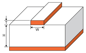
Fig. 1:- Track width and height (Thickness of copper sheet) over the base material
Fig. 1 shows the common structure of a PCB laminate and width and height relationship of the copper foil.
This relationship is for dc resistance calculation of the track without considering the copper on another layer.
The thickness of a track over a laminated sheet ranges from 17µm to 70µm unless specified otherwise.
The resistance relations show that the resistance is directly proportional to the length of the track, i.e., the longer the route, the higher the opposition, and vice versa.

The crosses sectional area is related to the width and height of the conductor. The manufacturer fixes the conductor thickness, and the width is the parameter controlled and varied by the PCB designer or manufacturer.
The track cross-sectional is
The A = cross-sectional area in (m2)
W = width of the track laid on the PCB
T = Height of the conductor, i.e., copper sheet thickness
These are the DC resistance parameters for a conductor. The voltage drop across a track due to dc resistance is:
Changes the track resistance significantly. This IR drop entirely causes heat dissipation. A Trace Width Calculator available online, offline in the form of excel sheets, or built-in design tool determines.
The width of the conductor at room temperature and elevated temperatures. The chart shows the same things, i.e., the cross-sectional area or thickness of the conductor, current, and temperature rise as in fig. 2.
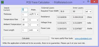
Fig. 2:- Screenshot of PCB trace width calculator with temperature compensation
PS: For example, the IRDrop analysis tool built into allegro signal integrity tools analyzes the analysis.

The width calculation, temperature analysis, and current density in the respective layout design. Track width vs. amperage charts is available easily. But calculators which accompany the temperature effect have better results, particularly in signal integrity analysis.


