Contents
- 1 What is a 10-layer PCB?
- 2 10-layer pcb stackup
- 3 10 Layer PCB Applications
- 4 The 10-layer board manufacturing process
- 5 10-layer pcb materials
- 6 How do you electroplate the 10-layer PCB stack?
- 7 How does 10 Layer PCB work?
- 8 How to Connect the 10-Layer PCB’s Signal Layers
- 9 10 Layer PCB advantages
- 10 Ten Layer pcb disadvantages
- 11 The Standard 10-layer PCB Stackup Dimensions
- 12 10-layer PCB Stackup Storage Conditions
- 13 How Do You Test the 10-layer PCB stackup?
- 14 circuit board repair
- 15 10 layer pcb manufacturers
- 16 Board thickness: How thick is a 10-layer PCB?
- 17 Summary
What is a 10-layer PCB?
A 10-layer PCB is a printed circuit board that has 10 layers of conductive material. Plus, this type of board is applicable for high-density applications where multiple signals need to be routed close together.
Moreover, 10-layer PCBs are common in high-speed applications where the extra layers allow for better signal integrity.
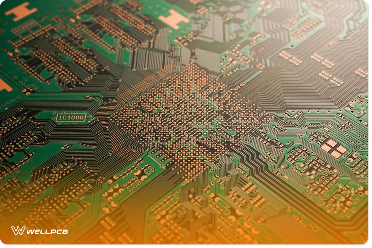
10-layer pcb stackup
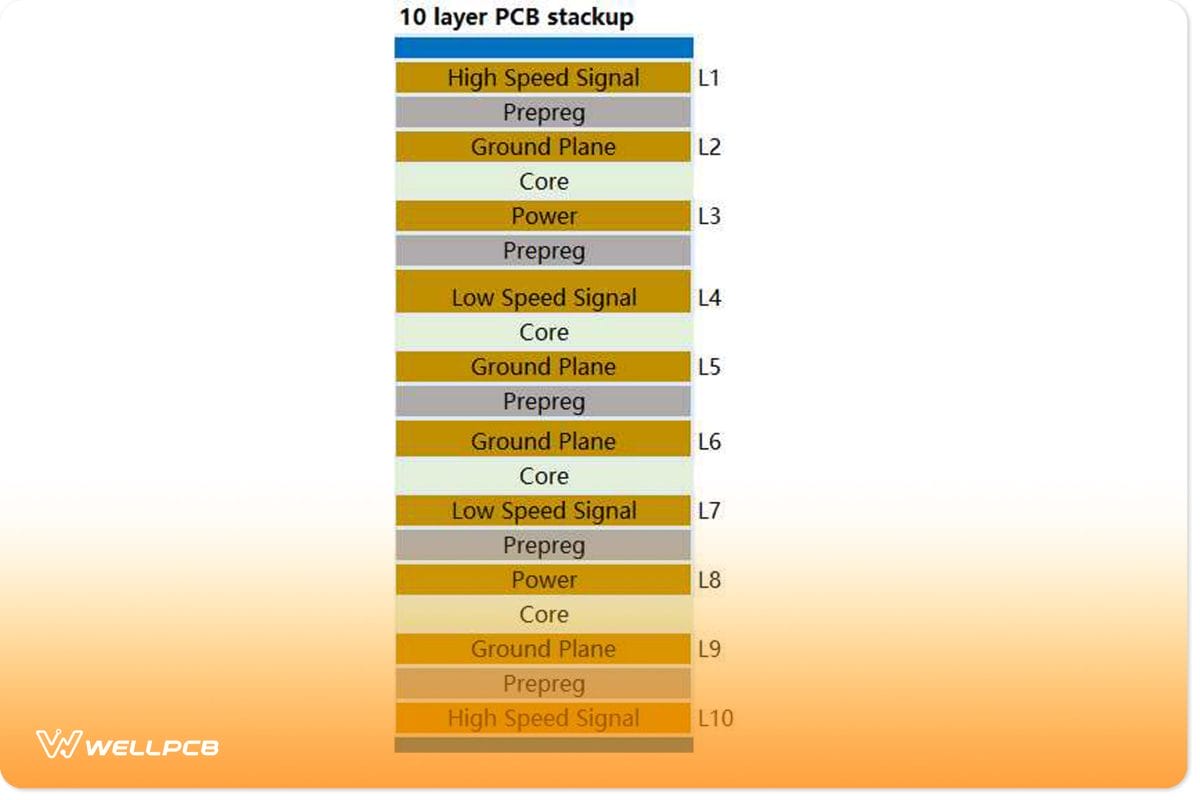
10-layer pcb stackup
The picture above shows the 10-layer pcb stack up. There are six signal layers /routing layers (high-speed and low-speed signals ) and four planes. The Bottom and top are the solder masks. Plus, the copper layers help to control the impedance, and it provides a return path for the signal. While the plane layers help to distribute the power and ground.
The six signal layers are for signal transmission. And low-frequency signals are in the outer layers, and high-frequency signals are in the inner layers. Without the signal layer, the PCB would be a short circuit.
The four plane layers are for power and ground distribution. The most commonly used are the inner two layers for power distribution and the outer two layers for ground.
The last two layers are the solder mask which is to protect the PCB from being shorted by solder, and the silkscreen, which is for component identification.
10 Layer PCB Applications
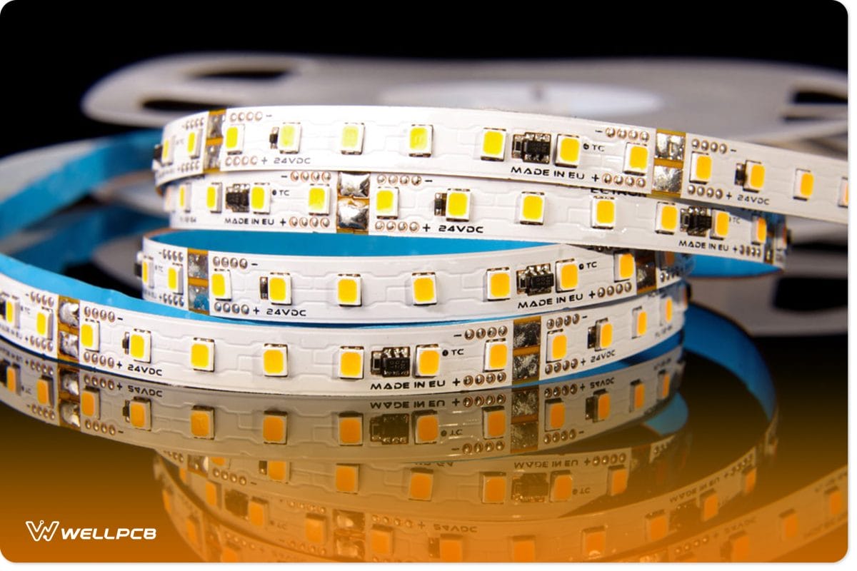
Light-emitting diode flexible PCB strip for various lighting applications
Many applications in a variety of sectors employ ten layers. The major goal of utilizing the circuits is to minimize signal loss. The following are some of the uses of 10-layer PCBs.
-Medical industry

Implantable cardiac pacemaker devices such as ICD and CRT devices are placed along with a stethoscope.
Medical electronics have to be extremely precise. Therefore, 10-layer PCBs are applicable in medical devices, such as pacemakers and other life-saving devices. Moreover, the 10-layer board provides the necessary space to place all of the required components while ensuring there is no signal loss.
-Space industry

Cargo spaceship on the orbit of planet Earth.
The space industry also takes advantage of 10-layer PCBs. For example, they are useful in satellites/satellite dishes and other spacecraft that need to function properly in extreme conditions. In addition, 10-layer boards are also resistant to radiation, making them ideal for space applications.
-Telecommunication industry

Telecommunication Tower and Telephone Transmitter and high voltage pole
The 10-layer PCB is also common in the telecommunication industry. For instance, they are applicable in base stations, sand storage, and other telecom equipment. Besides, they are also useful in mobile phone applications, laser direct imaging, and the memory module industry.
-Consumer electronics

Digital camera the night view of the city
10-layer PCBs are also applicable in a variety of consumer electronics. For example, they can be found in digital cameras, camcorders, and DVD players. In addition, 10-layer boards are common in laptop computers, mobile broadband routers, and LCD TVs.
-Automotive Industry
engine control unit macro style
You can also use the 10-layer PCB in automotive. For instance, they are applicable in engine control units, automotive dashboards, and other electronic control systems. In addition, 10-layer boards are also useful in navigation systems and infotainment systems.
-Industrial Processing Industry
Also, you can use 10-layer PCBs in a variety of industrial processing applications. For example, they can be found in process control systems and machine vision systems. In addition, 10-layer boards are also common in motion control systems and robotics applications.
-Military and Defence Industry
10-layer PCBs are also good in military and defense applications. For example, they can be useful in missile guidance systems and radar systems. In addition, 10-layer boards are also common in satellite communication systems and night vision systems.
In every one of these industries, 10-layer PCBs are being applied in a variety of ways. These will help ensure that the devices work at an optimum level and provide the best performance.
The 10-layer board manufacturing process
The 10-layer board fabrication is not very different from the process of manufacturing other types of PCBs. In general, the fabrication process involves several steps, including:
- Creating the circuit design
- Transferring the circuit design to a board
- Etching the copper traces
- Applying solder mask and silkscreen
- Assembling the components
- Testing the circuit boards
10 layer pcb
10-layer pcb materials
New Produced Automotive PCB with Soldered Surface Mounted Components.
The 10-layer pcb is made of different materials, including:
- Copper
- Solder mask
- Silkscreen
- FR-40 dielectric material
- Polyimide or Teflon substrate
These materials are for the specific properties that make them ideal for 10-layer PCBs. For example, the FR-40 dielectric material has a very low dielectric constant, which is important for 10-layer PCBs because it minimizes signal crosstalk between the different layers.
How do you electroplate the 10-layer PCB stack?
Firstly, you plate the 10-layer PCB with a thin layer of copper. And then, this is followed by a layer of solder mask, which you will apply to both sides of the PCB. The silkscreen is then in use on the top side of the PCB. Finally, you use the FR-40 dielectric material and polyimide or Teflon on the bottom side of the PCB.
The 10-layer PCB is then ready for assembly. First, you place the components on the top side of the PCB and solder them in place. Then, fill the through-hole vias with solder and coat the bottom side of the PCB with a solder mask. The 10-layer PCB is then ready for testing.
How does 10 Layer PCB work?

PCB Technology Information Pattern Concept Vector Background.
The working principle of a 10-layer PCB is very simple. As you know, a 10-layer pcb consists of 10 thin layers of copper foil laminated together. These 10 thin layers are separated by an insulating material known as the substrate. Also, the manufacturers are connecting 10 thin layers to each other through vias (plated-through holes). Then, they coat the 10-layer pcb with a solder mask, which is a protective layer.
How to Connect the 10-Layer PCB’s Signal Layers
Flex printed circuit boards with a copper layer in man fingers isolated on black background.
The 10-layer PCBs have two methods of connecting the signal layers:
– The first one is through the use of micro vias. In this method, you should drill the 10-layer PCB with small holes (micro vias), which are then filled with copper and plated over. You may use the method when the 10-layer PCB needs to have a high density of interconnections.
– The second method is through the use of blind vias. In this method, first, drill the 10-layer PCB with small holes (blind vias), which are then filled with copper and plated over. This method is in use when the 10-layer PCB needs to have a high density of interconnections but only on one side of the board.
Both methods have their advantages and disadvantages, so it is important to choose the right method for your 10-layer printed circuit board project.
10 Layer PCB advantages
A close-up of black Green colored PCB with no component mounted (copper exposed)
10-layer printed circuit board stack-ups have a number of advantages in the technical realm.
You will also appreciate working with the 10-layer PC stackups’ excellent performance outcomes.
The ten-layer PCB stack-ups have the following advantages.
-Light in Weight
Computer board in the hand of a man. Small PCB close-up.
The 10-layer PCB is thinner and lighter in weight as compared to the other types of boards. This is because the 10-layer stackup uses fewer materials, which, in turn, reduces the overall weight of the board. As a result, this makes it easy to carry and install 10-layer PCBs.
-Reduced Cost
The 10-layer stack-up is less costly as compared to the other types of multilayer boards. This is because it uses fewer materials, which in turn reduces the overall manufacturing costs.
-Better Flexibility
10-layer pcb manufacturers offer 10-layer boards in a variety of sizes, shapes, and colors. Hence, this gives you the freedom to choose the 10-layer PCB that best suits your needs.
-Better performance

Microchip production factory Hitech industry background
the pcb manufacturers offer 10-layer boards with improved performance. The 10-layer stack-up provides better heat dissipation, which in turn improves the overall performance of the board.
-Increased Power

holes in the circuit boards and contact pads
The manufacturers offer 10-layer boards with increased power density. As a result, the 10-layer stack-up provides better heat dissipation, which in turn increases the overall power density of the board.
Ten Layer pcb disadvantages
Photo of the electric component in an electronic device.
There are several benefits to using a 10-layer PCB stack-up, but you may be concerned about the drawbacks. But, as you may imagine, ten-layer PCB stack-ups aren’t quite perfect. There are certain limitations.
Here are some of the drawbacks of 10-layer PCB stack-ups that you should be aware of.
-High Cost

Cost reduction business finance concept on virtual screen.
The 10-layer stackup is the most expensive type of printed circuit board. The high cost is due to the increased number of layers and the increased complexity of manufacturing.
-Limited Availability
There are fewer 10-layer PCB manufacturers than there are for other layers of printed circuit boards. And this is because the 10-layer stackup is more complex to manufacture than other types of PCBs.
-Higher Risk of Manufacturing Defects
The 10-layer stackup is more complex than other types of PCBs, so there is a higher risk of manufacturing defects. These defects can include shorts, open circuits, and incorrect dimensions.
-Require Specialized Equipment

Electronic industry. Shop production of printed circuit boards.
The 10-layer stackup requires specialized equipment for manufacturing. This specialized equipment includes laminates, drills, and plating processes.
– Production Time Is Longer
The 10-layer stackup is more complex and requires more time to manufacture. In fact, the production time for a 10-layer PCB can be up to 10 times longer than other types of PCBs.
– Skilled Design Requirement

Electrical Engineers Work on Computer with CAD Software.
To construct the 10-layer PCB stackup, you’ll need skilled designers who have extensive knowledge of the design process.
In this scenario, the problem is a lack of availability or scarcity of such designers, which raises demand and pricing.
The Standard 10-layer PCB Stackup Dimensions
There are two standard 10-layer PCB stack-up dimensions: board thickness: 10-mil and 12-mil.
The 10-mil stack-up is the most common. The 10-mil stackup has a total board thickness of 0.04 inches (or 10 mm), and the 12-mil stackup has a board thickness of 0.048 inches (12 mm).
You can also find 10-layer PCBs with a 14-mil or 16-mil board thickness, but those are less common. The 10-layer stackup dimensions are as follows:
- 10-mil: 0.04 inches (or 10 mm)
- 12-mil: 0.048 inches (12 mm)
- 14-mil: 0.0551 inches (14 mm)
- 16-mil: 0.0635 inches (16 mm)
The 10-layer stackup is the most popular because it offers the best balance of rigidity and flexibility. Plus, it’s also the thinnest option, which makes it the lightest and most economical.
If you need a more rigid board, you can choose the 12-mil stack-up. This option is a bit thicker and heavier, but it’s more resistant to warping and bending.
The 14-mil and 16-mil stack-ups are less common because they’re thicker and heavier, which makes them more expensive. They’re also more prone to warping and bending.
10-layer PCB Stackup Storage Conditions
PCB Board manufacturing and testing process
When it comes to ten-layer PCBs, you’ll need to take extra care when handling and storing them.
– Make sure to store them in an anti-static bag and at room temperature.
– Also, avoid exposing them to sunlight.
– If you have to transport them, do so in an anti-static bag as well.
With these simple tips, you’ll be able to keep your 10-layer PCBs in good condition for a long time.
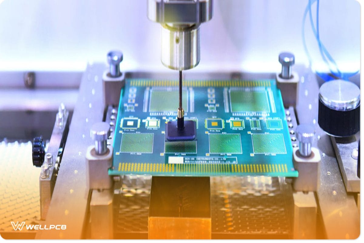
How Do You Test the 10-layer PCB stackup?
PCB Processing on soldering iron tips of automated manufacturing soldering and assembly pcb board
When you’re ready to test your 10-layer PCB stackup, there are a few things you’ll need to do.
First, make sure all the layers are aligned correctly. You can do this by using a layer alignment tool.
Next, connect all the layers using an adhesive or solder mask.
Finally, test the stackup by running a current through it. You can do this by using a multimeter or an oscilloscope.
If everything checks out, you’re ready to move on to the next step in your project! If not, make sure to fix any errors before proceeding.
circuit board repair

The engineer Does Computer Motherboard Soldering.
As your 10-layer PCB stackup ages, you may find that some of the layers start to separate. This is normal, and you can fix it with a simple circuit board repair kit.
First, identify which layer is affected. Then, use the adhesive or solder mask to reattach the layer. Finally, test the connection to make sure it is secure.
With a little bit of care, your 10-layer PCB stackup will last for years to come!
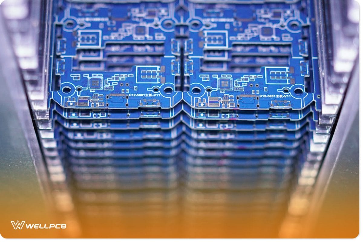
10 layer pcb manufacturers
Technological process of soldering and assembly chip components on pcb board. Automated soldering machine
It is no secret that 10-layer PCBs are complex and expensive. That’s why it’s so important to choose the right 10-layer PCB manufacturer for your project. Here are a few things to keep in mind:
– Capacity:
Make sure the manufacturer you choose has the capacity to handle your project. 10-layer PCBs are complex and require a lot of resources.
– 10 Layer PCB Manufacturer: Experience:
10-layer PCBs are not for the faint of heart. Make sure the manufacturer you choose has experience with this type of project in the pcb industry.
– Quality:
10-layer PCBs are expensive. You want to make sure you’re getting the best quality for your money.
– Customer service:
Make sure the 10-layer PCB manufacturer you choose has great, efficient service to help you with any questions or issues that may arise. Besides, online customer support.
-10 Layer PCB Manufacturer: pcb prototype
Whether your manufacturer will offer you a pcb prototype service is another important factor to consider. A pcb prototype can help you catch errors and design issues early on, saving you time and money in the long run.
-lead time
On-time delivery is crucial in the electronics industry. Make sure to ask your pcb manufacturer about their manufacturing time and if they can meet your deadlines. Also, the flexible shipping methods.
-10 Layer PCB Manufacturer: competitive rates
Getting high-quality products at the best price is the key to success. One-stop solution pcb manufacturers with competitive rates will help you save money and get the most bang for your buck.
-10 Layer PCB Manufacturer: minimum orders
Be sure to ask your pcb manufacturer about minimum order quantities (MOQ) before committing to a purchase. Some manufacturers have high MOQs that could end up costing you more in the long run.
Do your research and choose the 10-layer PCB manufacturer that’s right for you and your project. With the right manufacturer, 10-layer PCBs can be a great addition to your product.
Board thickness: How thick is a 10-layer PCB?
blue electronic PCB boards assembled at an SMT factory and put together in a rack
The thickness of a ten-layer PCB can vary depending on the manufacturer and the materials used. Generally, 10-layer PCBs are between 0.06 inches (0.15 cm) and 0.09 inches (0.23 cm).
When choosing a professional pcb manufacturer, be sure to ask about the finished board thickness and what materials they will use. This will ensure that you get the right board for your project.
With the right PCB manufacturer, you can get a great addition to your product. Do your research and choose the one that’s right for you and your project. With the help of customer service, you can be sure to have any questions or concerns answered so that you can get the 10-layer PCB that’s perfect for your needs.
Summary
The PCB manufacturing process is not as simple as it may seem. It’s important to select the right manufacturer and understand the entire process so that your PCB project goes smoothly. By taking into account all of the factors involved in PCB production, you can be sure that your boards are manufactured correctly and delivered on time. Have you ever worked with a PCB manufacturer before? What was your experience like? Let us know in the comments below.
What are some other things to keep in mind when choosing a PCB manufacturer? Share your thoughts in the comments below. Thanks for reading!