Contents
- 1 What is an 8-layer PCB?
- 2 Why You Should Use The 8-Layer PCB stack up
- 3 8-layer PCB stack-up Materials
- 4 8-layer PCB stack-up applications
- 5 8-layer PCB Stack-up Benefits
- 6 8-layer PCB stack up
- 7 8-layer PCB thickness
- 8 Grounding rules for multilayer PCBs-8 layer PCB
- 9 8 Layer PCB Prototype
- 10 What is the Difference Between the 4 Layer PCB Stackup and the 8 Layer PCB Stackup?
- 11 6-layer vs 8-layer PCB
- 12 Standard 8 Layer PCB Stack-up Manufacturing Techniques
- 13 Cost Factors that Influence 8-Layer PCB Stackups
- 14 8-layer PCB stack up manufacturer
- 15 multilayer printed circuit board
- 16 FAQs:
- 17 Summary
What is an 8-layer PCB?
Circut boards standing in a row
An 8-layer PCB is a printed circuit board that has 8 layers of conductive materials. These 8 layers are typically made of copper, and they will connect electronic components together. The 8 layers, which insulating materials separate them, and they get connection together by vias (holes).
A multilayer PCB with eight-layer, also known as an 8-layer PCB, has ample routing space and vias space for applications that require multiple power islands.
Why You Should Use The 8-Layer PCB stack up

High-tech electronic PCB with the processor, microchips, and glowing digital electronic signals
To improve EMC performance, 8 layer PCB is necessary in some cases
* 8-layer PCB can provide better EMC shielding than lower layer count boards.
* 8-layer PCB can provide better power and ground plane separation than lower layer count boards.
*The 8-layer PCB can provide more routing layers than lower layer count boards.
* 8-layer PCB can provide better high-speed signal routing than lower layer count boards.
8-layer PCB stack-up Materials
Detail of an electronic printed circuit board with many electrical components
8-layer PCB comprises a stack of alternating dielectric and conductive layers. The most common materials used in 8-layer PCB are:
Conductive Materials:
* Copper
Copper is the most common material useful in 8-layer PCB. Besides, it is an excellent conductor of electricity and has a relatively low cost. Also, the cost of recycling copper is very low.
* Gold
Gold is a less common conductive material useful in 8-layer PCB. In addition, It is an excellent conductor of electricity and has a relatively high cost.
* Silver
Silver is a good conductor of electricity and does not corrode. And it is less expensive than gold.
* Aluminum
Aluminum is a good conductor of electricity and has a relatively low cost. However, aluminum tends to corrode.
Aluminum 8-layer PCB is to carry high current traces. In addition, these traces are typically very thick and have a low impedance.
Printed circuit board and microchip
Substrate materials
Heat and signals both get insulated by using an insulating material, such as glass-epoxy materials. In addition, 8-layer PCB is also in use to carry high current traces. And these traces are typically very thick and have a low impedance.
Dielectric Materials:
* Polyimide
Polyimide is a common dielectric material useful in 8-layer PCB. Plus, it has a very low dielectric constant and loss tangent.
* FR-408
FR-408 is another common dielectric material useful in 8-layer PCB. Besides, it has a lower dielectric constant and loss tangent than polyimide.
* Rogers RO400
Rogers RO400 is a dielectric material that has a very low dielectric constant and loss tangent. Also, It’s common to find 8-layer circuit boards.
* Arlon AD2000
Arlon AD2000 is a dielectric material that has a very low dielectric constant and loss tangent. In addition, the 8-layer PCB is standard.
Many other dielectric materials can use 8-layer PCB, but these are the most common. When choosing a dielectric material 8-layer PCB, it is essential to consider the dielectric constant, loss tangent, and thermal conductivity.
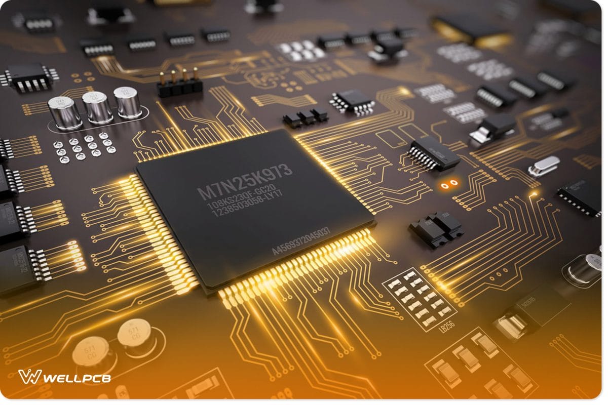
8-layer PCB stack-up applications
High frequency printed circuit board PCB
8-layer PCBs are most commonly applicable in high-frequency applications where signal integrity is important. Besides, 8-layer PCB can also get used in applications where thermal conductivity is important. Some common 8-layer PCB applications include:
– High-Speed Digital Boards
– RF & Microwave Boards
– Power Amplifier Boards
– Thermal Management Solutions
– LED Lighting Boards
8-layer PCB Stack-up Benefits

Assembling a circuit board
There are many benefits to using an 8-layer PCB over the lower layer circuit board. Here is a list of the advantages.
Reduce Radiation
Emission: 8-layer PCB has better signal integrity that helps to reduce radiation emission.
Improved Power Distribution:
8-layer PCB can provide improved power distribution with the help of inner layers.
Increased Reliability
Compared to the lower layer circuit board, the 8-layer PCB is more reliable because of the improved power distribution and signal integrity.
Cost-Effective
The 8-layer PCB is more cost-effective than lower layer circuit board because it uses less material and is more efficient to manufacture.
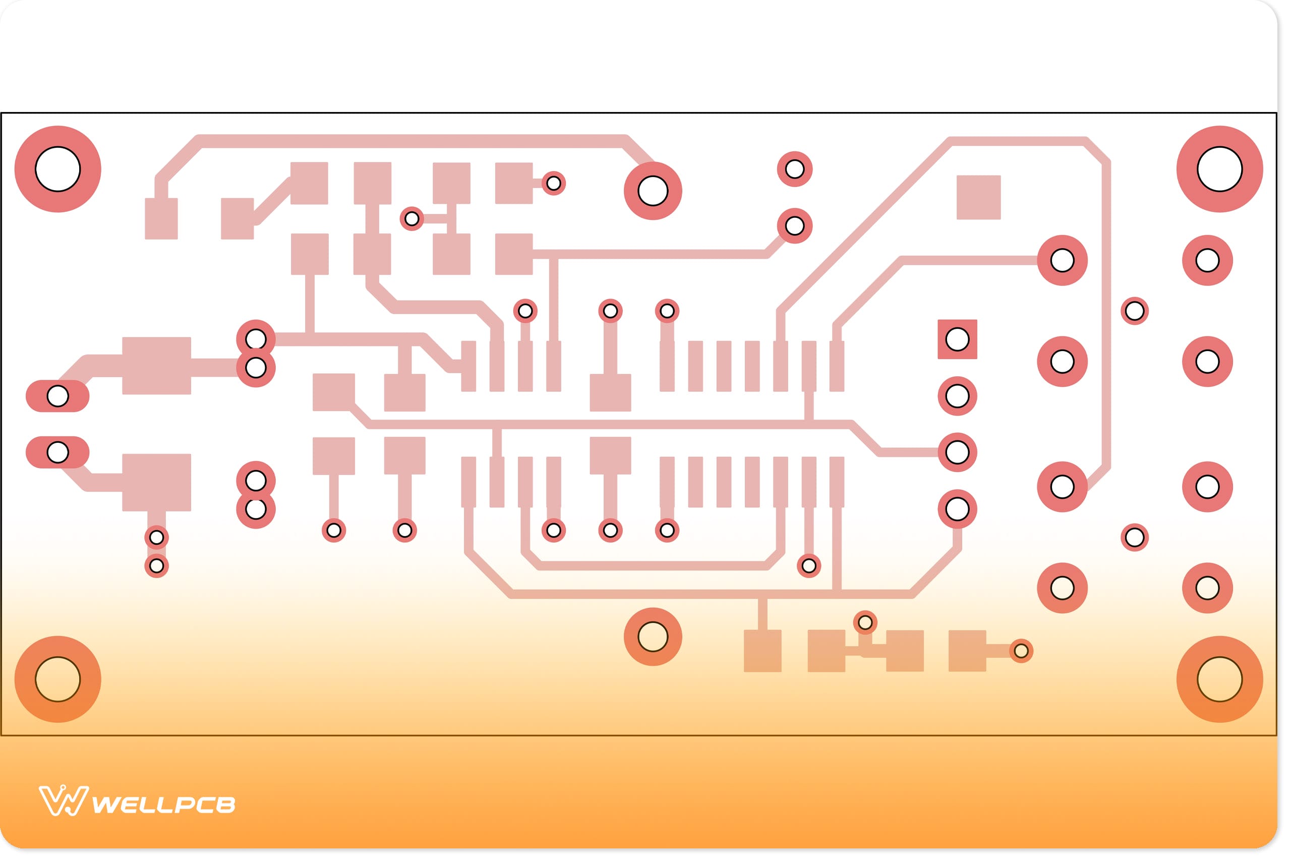
8-layer PCB stack up

8-layer PCB stack up
The typical 8-layer PCB stack-up usually contains:
Top and bottom layers, four signal layers, four plane layers, solder masks, core, and prepreg.
Signal Layers:
* Inner Layers
The inner layers of 8-layer pcb get applicable to carry signal traces. And these traces are typically very thin and have a high impedance.
* Outer Layers
The layers of 8-layer PCB are in use to carry signal and ground traces. Furthermore, these traces are typically very thin and have a high impedance.
Ground Layers:
* Inner Layers
The inner layers of 8-layer pcb are good to carry ground planes. Moreover, these planes are typically very large and have a low impedance.
* Outer Layers
The outer layer of the 8-layer PCB gets applied to carry power and ground signals. In addition, these signals are typically low-frequency and have a high current carrying capacity.
Power Layers:
* Inner Layers
The inner layers of an 8-layer PCB are to carry power signals. Also, these signals are typically high-frequency and have a low current carrying capacity.
* Outer Layer
The outer layer of 8-layer pcb is useful for carrying power and ground signals. Also, these signals are typically high-frequency and have a low current carrying capacity.
Here are the details of all the layers:
*Top layer
This is also the high-speed signal layer. And the routing is on the top and bottom of this layer. The vias are also in connection to this layer.
*Layer 2
This layer is GND Plane or ground layer, ground plane layer. Plus, It is for the power and ground of high-speed signals.
*Layer 3
This layer is also also the high-speed signal layer.
*Layer 4
This layer is GND Plane or ground plane layer.
*Layer 5
This layer is GND Plane or ground plane layer.
* Layer 6
This is also the high-speed signal layer.
*Layer 7
This layer is GND Plane or ground plane layer.
*Bottom layer
This layer is also also the high-speed signal layer.
Note that signal layers get separated by ground and power planes to reduce EMI susceptibility and emission.
Besides that, core material and prepregs used in 8-layer PCB are also important. Plus, Rogers RO4350B and Tachyon 855 are good choices for 8-layer PCB.
In addition, impedance control is important for transmission line design and the thickness and composition of materials may have an impact.
8-layer PCB thickness
Chips on a blue PCB
The thickness of an 8-layer PCB can vary, depending on the manufacturer. However, the average thickness is about 0.060 inches (0.1524 cm). This thickness is necessary to accommodate all 8 layers of conductive material, as well as the insulating materials between them.
Grounding rules for multilayer PCBs-8 layer PCB
- Firstly, do not cut the bottom layer.
- Secondly, drill the vias as small as possible.
- Thirdly, place the vias away from sensitive areas. Also, keep the via length as short as possible.
- Fourthly, make sure nothing is left unattended.
- Fifthly, don’t forget about the return current path.
- Sixthly, place the ground planes as close to each other as possible.
- Last but not least, check the impedance.
If you follow these simple 8-layer PCB grounding rules, your board will be well on its way to success!
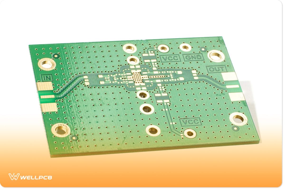
8 Layer PCB Prototype
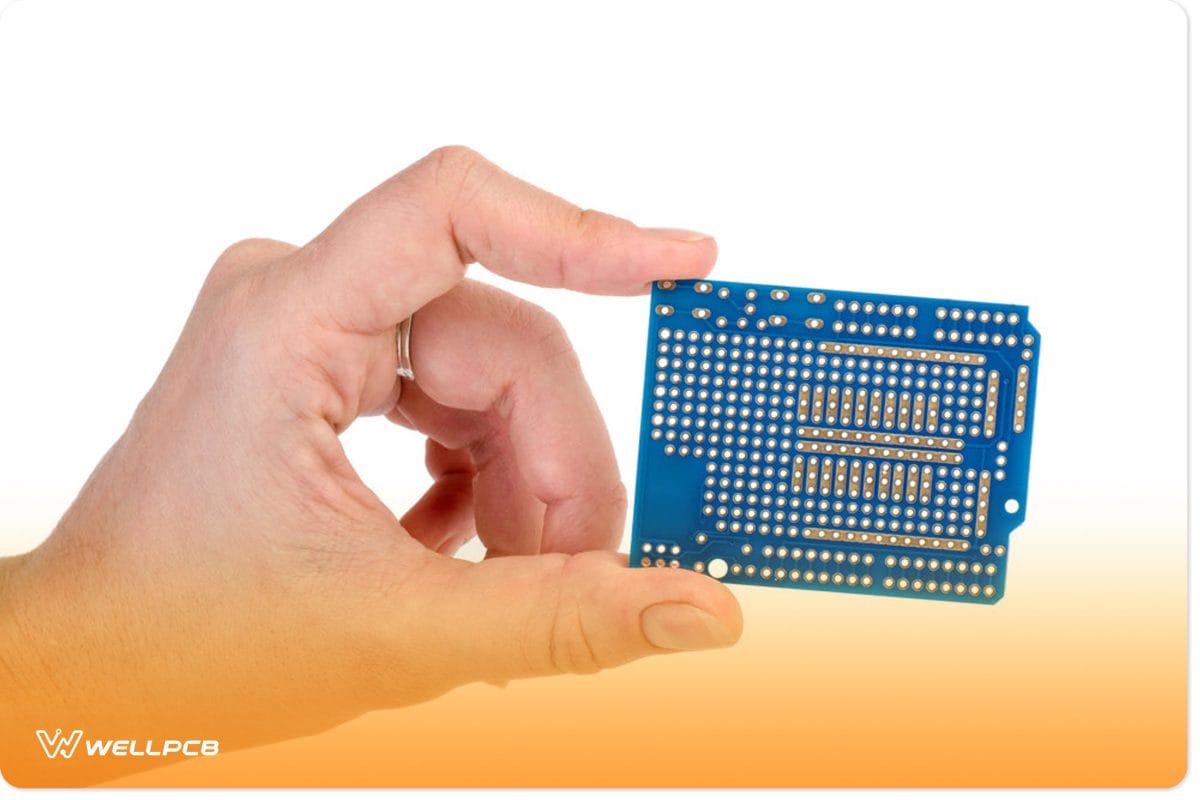
Blue prototyping PCB in a hand
The 8-layered FR-4 PCB Prototype is a kind of printed circuit board with eight layers that get firmly linked together and have reliable connections mutually between them.
The FR-4 has more complicated structures than an 8-layer FR-4 PCB.
- Firstly, it creates more room for concealing transmitted signals from adjacent layer signals.
- Plus, to minimize noise coupling, it features multiple power and ground planes, as does a digital ground plane.
- In addition, isolation and impedance control on traces are necessary for analog signals, especially those with RF.
- Finally, using many more layers helps us route signals needing to be matched.
What is the Difference Between the 4 Layer PCB Stackup and the 8 Layer PCB Stackup?
The 8-layer stack-up is very similar to the 4-layer stack-up. However, the main difference is that there are two extra planes in the 8-layer stack up. Also, these extra planes can be in use for power or ground. Plus, the 8-layer stack up also has more vias than the 4-layer stack up.
6-layer vs 8-layer PCB
The main difference between a 6-layer and 8-layer PCB is the number of layers. In addition, an 8-layer PCB has two more layers than a 6-layer PCB. Plus, these extra layers can be in use for power or ground. Also, the 8-layer stack up has more vias than the 6-layer stack up.
Standard 8 Layer PCB Stack-up Manufacturing Techniques

Assembling a circuit board
As technology advances, the need for more sophisticated 8-layer PCB stackups becomes apparent in many applications. Furthermore, there are several challenges that we must overcome when designing 8-layer boards.
Signal integrity
Signal integrity is one of the most important aspects to consider when designing 8-layer PCBs. Additionally, you must design the stack up in a way that minimizes the risk of crosstalk and other signal integrity issues.
Direction of Routing
An 8-layer PCB stack-up might include six signal layers in some situations.
To minimize cross talks, you should route the adjacent layers’ signal traces perpendicular to one another.
Habitually subsequent layers route signal layers differently, though it may separate them by power or ground planes, to be safe.
Power delivery
Another important aspect to consider when designing 8-layer PCBs is power delivery. Also, you must design the stack up in a way that optimizes power delivery to the components on the board.
Thermal management
Thermal management is another important consideration when designing 8-layer PCBs. Therefore, you must design the stack up in a way that minimizes the risk of thermal issues.
Blind Vias or Buried Vias
You may also choose blind or buried vias to maximize the routing area. Furthermore, you should talk to your manufacturer about whether they can produce the component on the PCBs.
manufacturability
When designing 8-layer PCBs, it is important to consider manufacturability. Also, you must design the stack up in a way that is easy to manufacture.
Return Path
Even if the high-speed signal is on the inner layer, it is critical to picture their return route.
Make sure that the signals have solid return paths on every layer, starting from the outermost one.
Also, we can achieve this by keeping a ground plane around the signal or, if that’s not possible, by stitching vias.
cost
Cost is another important consideration when designing 8-layer PCBs. So you must design the stack up in a way that is cost-effective.
Ground Plane
Generally, since it might cause a discontinuity of impedance, it is essential to avoid having split ground planes
In addition, make sure the outside layer’s components are in connection to the ground planes of the inner layers via low-impedance vias.
Cost Factors that Influence 8-Layer PCB Stackups

Hardware testing
Manufacturing an 8-layer stack-up is expensive, and it has several components that add to the overall price. However, certain elements influence the cost.
Sizes of printed circuit boards
The size of the 8-layer PCB is the first cost factor to consider. Therefore, the larger the board, the more expensive it will be. This is because the boarding house will need to use more material, and the process of making the 8-layer stack up will take longer.
Pitch
The next cost factor is the pitch. Also, the pitch is the distance between the center of one via to the center of another via. So the smaller the pitch, the more vias that need to be drilled, and the more expensive the 8-layer stack will be.
Drill Size
The size of the drill also impacts the price. As a result, the smaller the drill, the more expensive it will be. This is because the boarding house needs to use a smaller drill bit, and the process of making the 8-layer stack up will take longer.
Copper Thickness
The copper’s thickness also impacts the price. The thicker the copper, the more expensive it will be. This is because the boarding house needs to use more copper, and the process of making the 8-layer stack up will take longer.
Surface finish types
There are a few different types of surface finishes, and each one impacts the price differently.
– HASL (Hot Air Solder Leveling) is the most common and the least expensive.
– ENIG (Electroless Nickel Immersion Gold) is more expensive because it’s a more complicated process.
– OSP (Organic Solderability Preservative) is less common and more expensive.
– Immersion Silver is less common and more expensive.
– Immersion Tin is less common and more expensive.
– Gold plating is the most expensive surface finish.
The price of 8-layer PCBs also depends on the features that are included. If you need buried or blind vias, for example, that will add to the cost. Specialized materials, like Rogers or Teflon, will also add to the price. Ultimately, the best way to get an accurate quote is to work with a reputable 8-layer PCB manufacturer. And they will be able to help you choose the right surface finish and features for your project.
8-layer PCB stack up manufacturer
What factors should you consider while picking a professional PCB manufacturer? There are a few things to think about.
– The 8-layer PCB manufacturer’s capabilities
Firstly, you need to consider the 8-layer PCB manufacturer’s capabilities. They should have the ability to produce 8-layer PCBs to your specifications. Also, you need to make sure that they have the necessary equipment and resources to produce 8-layer PCBs.
Whether they have advanced production lines, skilled workers, and 8-layer PCB design engineers.
In addition, the 8-layer PCB manufacturer’s expertise is essential. Hence, you should consider the 8-layer PCB manufacturer’s experience. They should have experience in manufacturing 8-layer PCBs so that they can produce a high-quality 8-layer PCB for you.
– 8-layer PCB manufacturing cost
The cost is also a concern. So you should have this in mind when looking for an 8-layer PCB manufacturer. The 8-layer PCB manufacturer’s cost will vary depending on their experience, 8-layer PCB technology, and 8-layer PCB size.
Besides that, your budget also needs to be considered.
– The 8-layer PCB delivery time
After you have considered the 8-layer PCB manufacturer’s experience and cost, you need to consider the 8-layer PCB delivery time. Because the 8-layer PCB delivery time is very important as you don’t want to wait too long for the 8-layer PCBs.
So, when looking for an 8-layer PCB manufacturer, you should consider their 8-layer PCB delivery time.
– 8-layer PCB technology
When looking for an 8-layer PCB manufacturer, you should also consider their 8-layer PCB technology. The 8-layer PCB technology is very important because it will.
multilayer printed circuit board
multilayer printed circuit board technology has come a long way in the last few years. The common types are double-layer PCB, 4-layer PCB, 6-layer PCB, 8 layer PCB. Also, you may find 10-layer stack up, 12-layer PCB stack up, and even 20-layer PCB stack up.
While the 8-layer PCB is now one of the most popular multilayers printed circuit board technologies. It is not always the best technology for your project. Hence you should also consider the 8-layer PCB delivery time when making your decision.
FAQs:
How many layers can a PCB have?
The short answer is “it depends.” And it depends on the project requirements.
How many layers of PCB do you need?
8 layers? 12 layers?
For most projects, 8 layer PCB is sufficient.
Summary
If you’re looking for a reliable and experienced 8-layer PCB manufacturer, look no further than our team. Our years of experience in the industry have taught us how to produce high-quality PCBs that meet your specific requirements. We understand the importance of quality and timely delivery, which is why we guarantee both with every order. Contact us today to get started on your next printed circuit board project!