Best PCB Assembly Manufacturing Service PCBA Company
WellPCB delivers comprehensive PCB assembly services, ideal for everything from low-volume PCB prototyping to high-volume board assembly manufacturing. We offer flexible production with no minimum order quantity and complete quality assurance.
- In-house SMT & THT assembly across dual ISO-certified factories with 13+ production lines.
- Full support for single/double-side SMT, mixed technology, and box build assembly.
- Flexible production from single prototypes to high-volume manufacturing

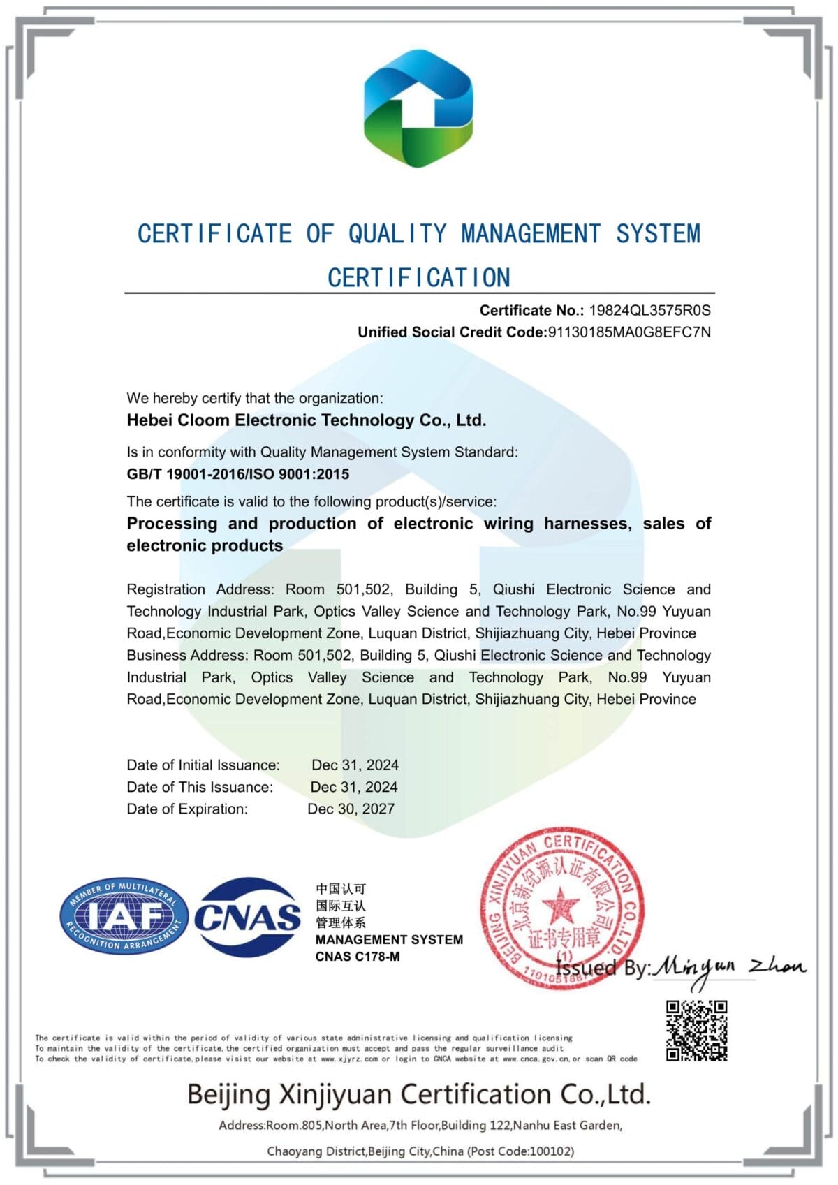
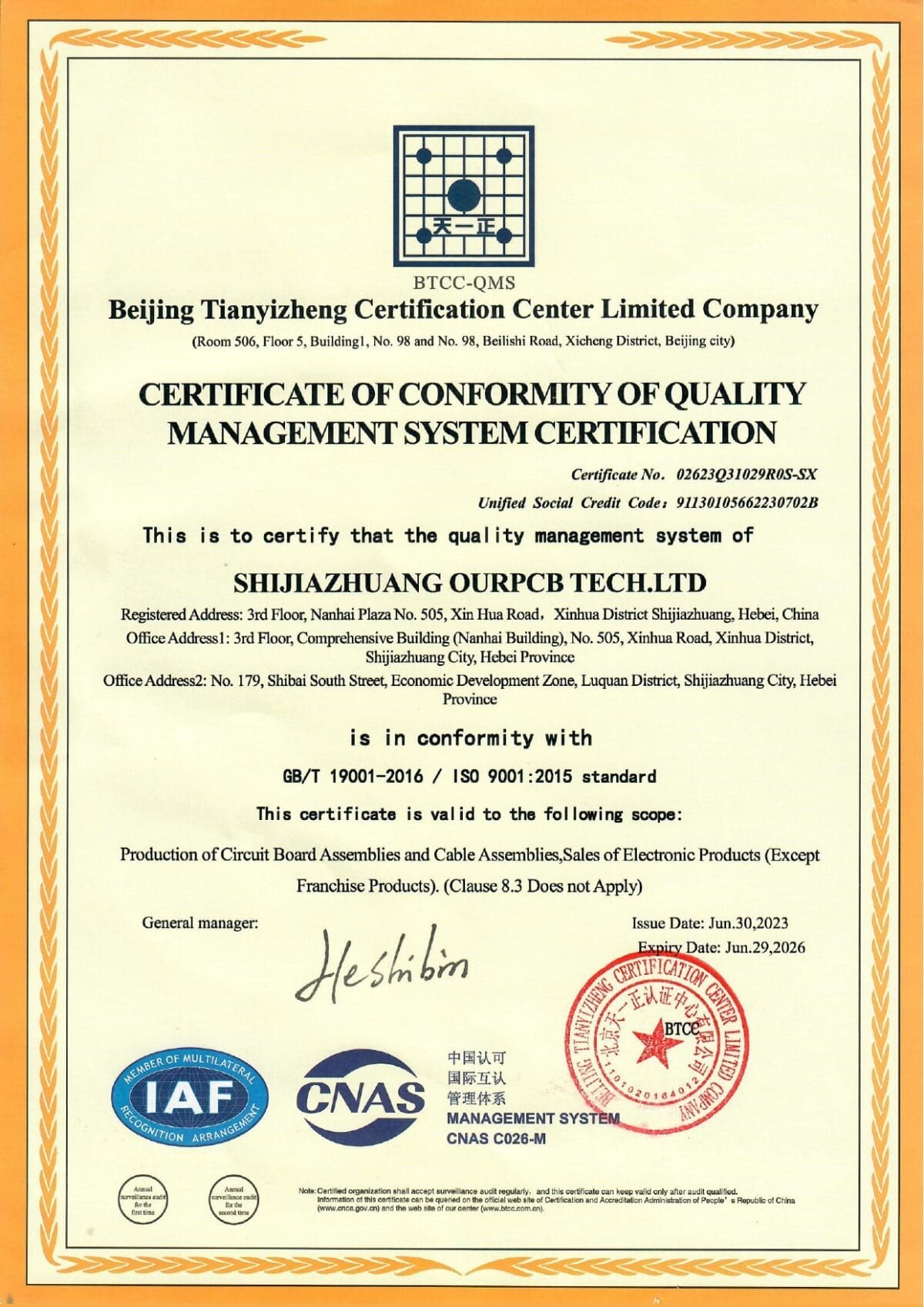
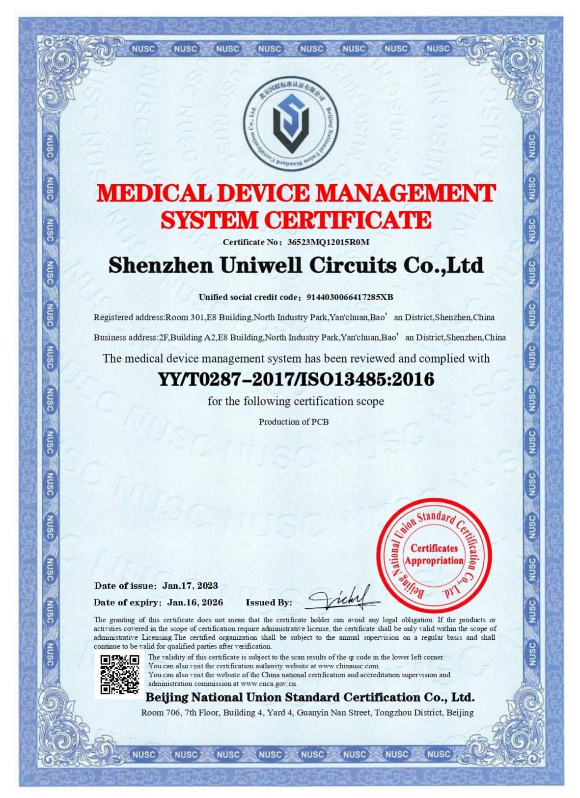
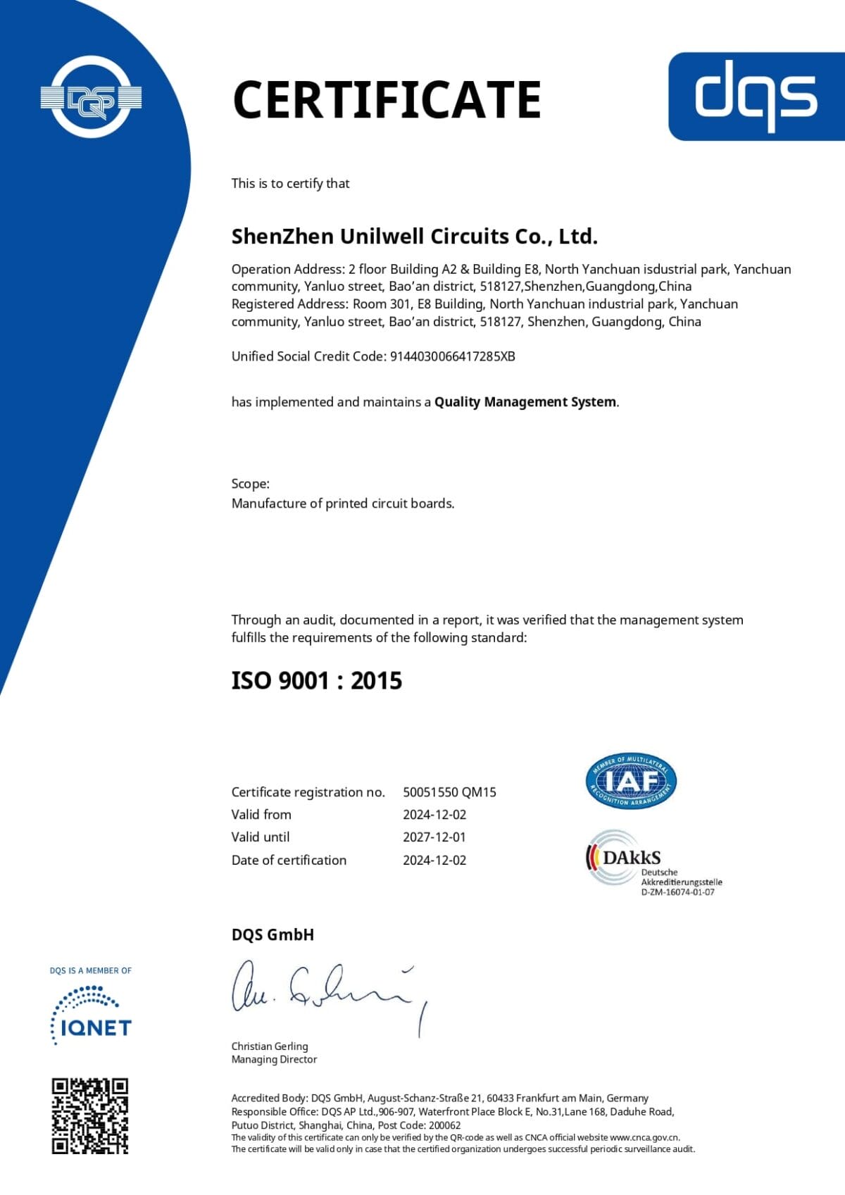
ISO9001 ISO13485
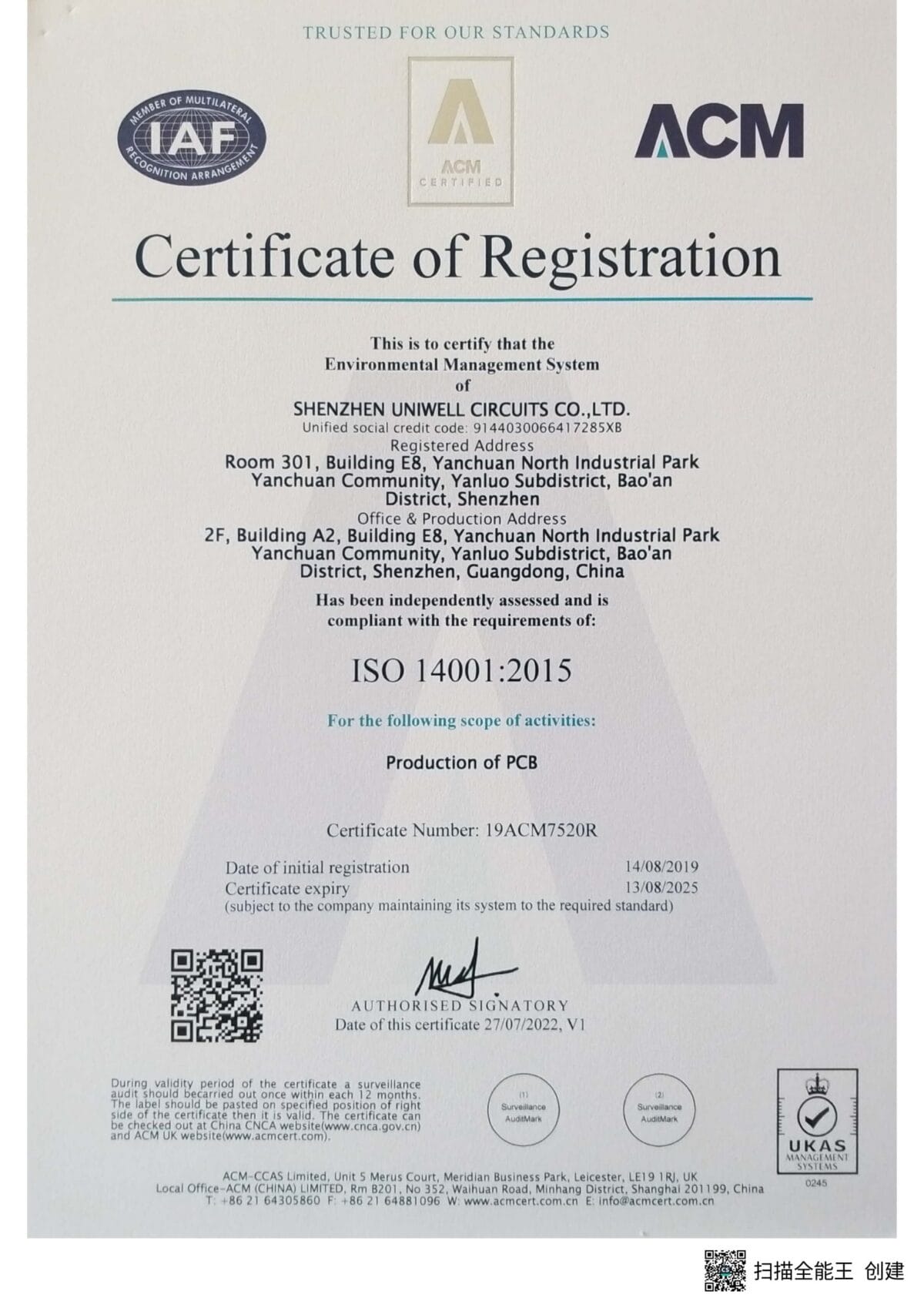
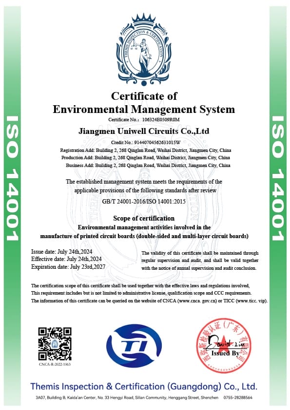
ISO14001

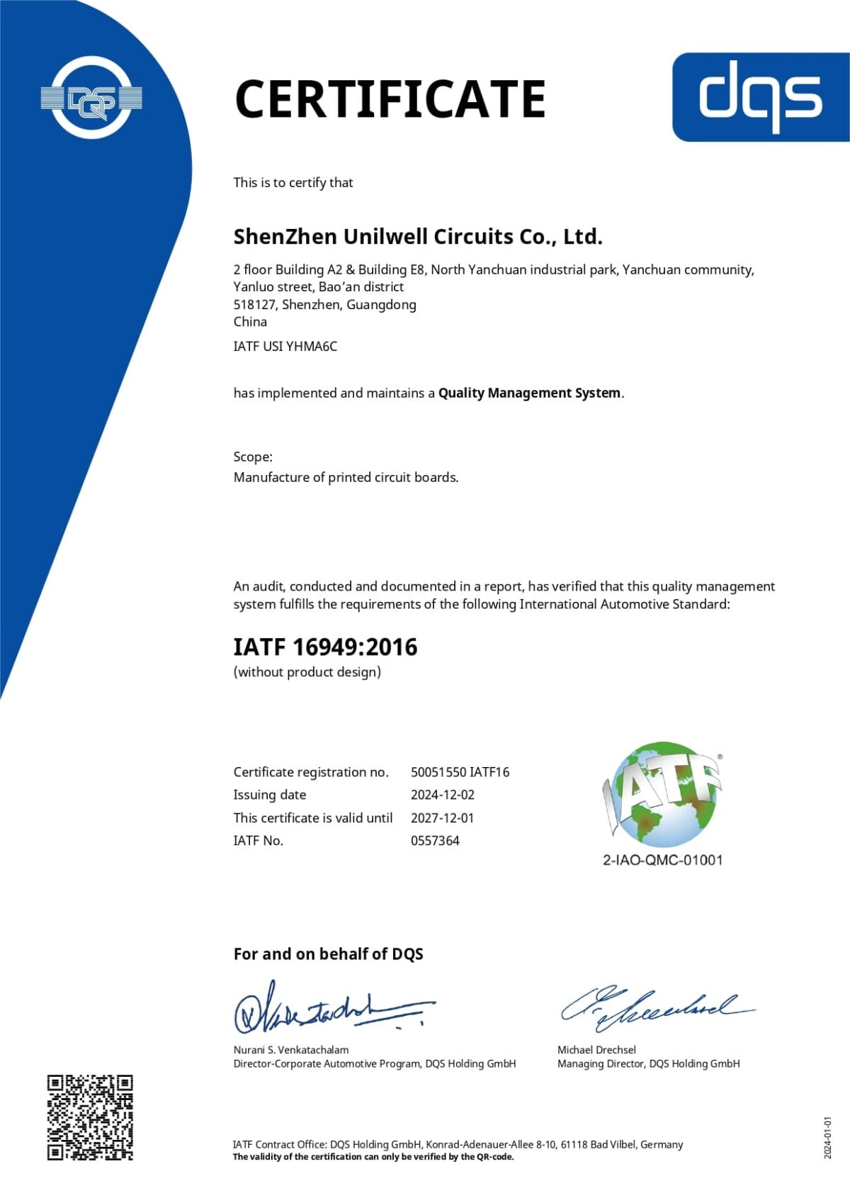
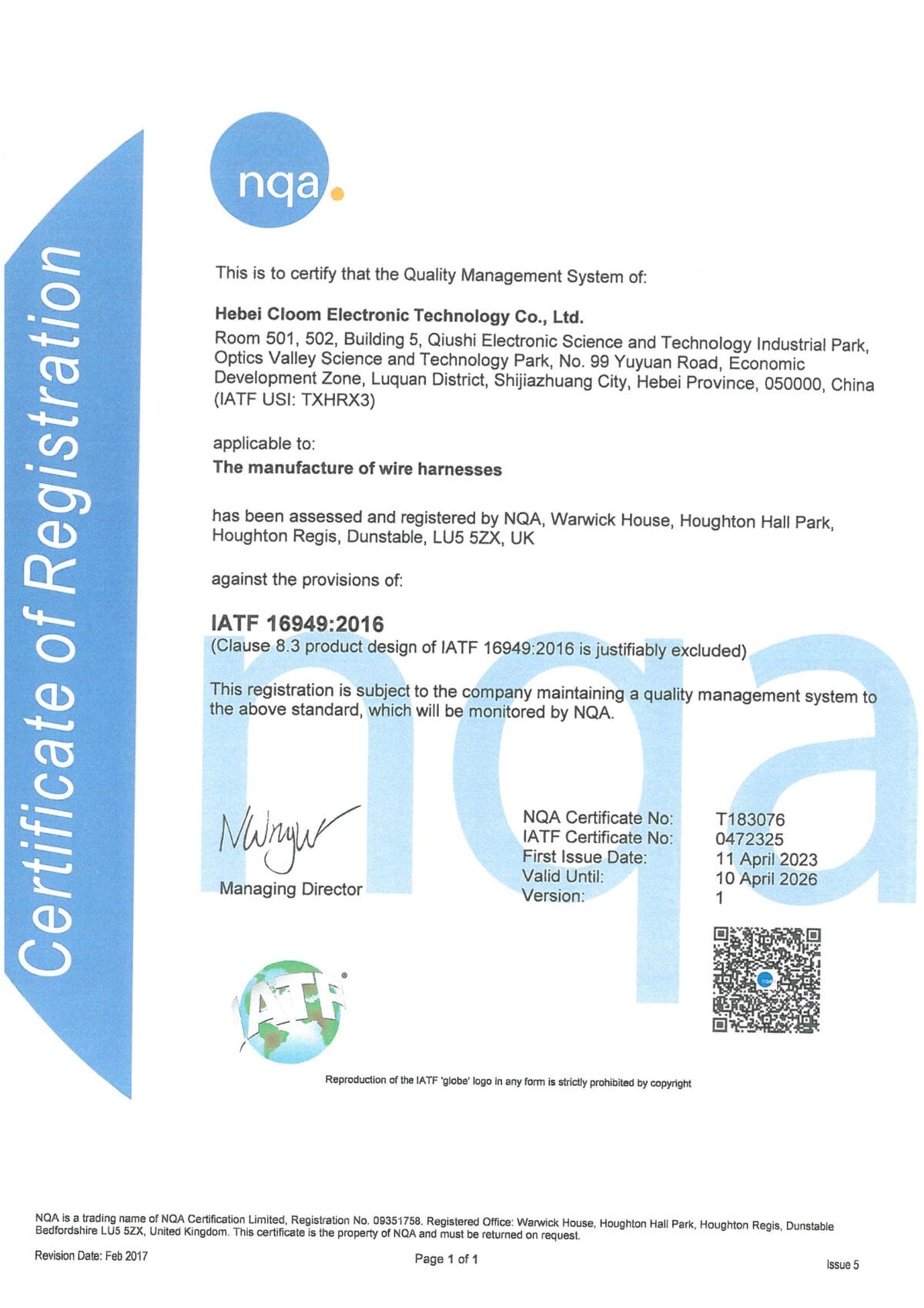
IATF
16949

IPC-A-610H International
Certification

Fully Automated
AOI Inspection
- PCB Manufacturer
- PCB Assembly Service
PCB Assembly Services
Built for Precision
WellPCB is a proven PCB assembly manufacturer offering a full range of services, including prototyping, fabrication, global component sourcing, surface-mount and through-hole assembly, post-solder inspection, and functional testing. With 18+ years of manufacturing experience, we deliver consistent, standards-compliant assemblies for lead-free (RoHS) and traditional soldering processes.
Our advanced assembly capabilities utilize SMT, through-hole, and hybrid assembly processes with full quality traceability throughout production. Our production lines handle fine-pitch BGA (0.2 mm) and QFP (0.15 mm) placements with <±30 µm accuracy and 60,000 CPH throughput capacity.
Our workflow is engineered for flexibility. We have no minimum order quantities and accommodate everything from single-board prototypes to volume PCB assembly. Every project benefits from in-house DFA checks, process traceability, and rigorous testing protocols that align with IPC-A-610 and ISO 9001:2015 standards.
All PCB assemblies undergo comprehensive testing including AOI, X-ray, ICT, FCT, solderability, thermal shock, and micro-section analysis to ensure compliance with ISO 9001:2015 and IPC-A-610 standards.
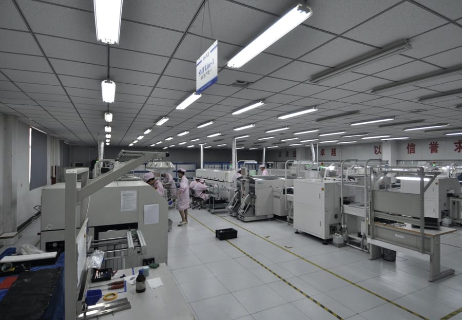
Our PCB Assembly Services Capabilities
| Feature | Specification |
|---|---|
| Maximum Placement Rate | 60,000 components per hour. |
| Equipment Used | 8 YAMAHA + 5 Siemens SMT lines across two facilities. |
| Component Types Supported | 01005, 0201, DFN, QFN, BGA, LGA, CSP, PoP, flip-chip. |
| Minimum BGA Pitch | 0.2 mm. |
| Minimum QFP Lead Width | 0.15 mm. |
| Placement Accuracy | ±30 µm @ 3σ (CPK ≥1). |
| Reliability Test | Flying Probe Test / Fixture Test, Impedance Test, Solderability Test, Thermal Shock Test, Hole Resistance Test, and Micro Metallographic Section Analysis, etc. |
| Reflow Profile Control | RoHS-compliant multi-zone convection with nitrogen reflow capability. |
| PCB Size Range | 50 mm × 50 mm to 610 mm × 508 mm. |
We support many assembly types, including single- and double-sided SMT, through-hole, and mixed technology assemblies.
Boards from 50 mm × 50 mm up to 610 mm × 508 mm are compatible, with thicknesses between 0.5 mm and 4.5 mm.
Component placement accuracy is maintained at <±30 µm (3σ) with CPK ≥ 1, allowing for reliable operation in high-density, tight-tolerance designs. Track widths down to 1.8 mil are supported for fine-line PCB layouts.
We support low-volume prototype assembly, pilot production, and high-volume PCB assembly with consistent process fidelity. Our facilities are optimized for both short-run agility and volume throughput.
WellPCB is certified to ISO 9001:2015 and ensures all processes align with IPC-A-610 Class 2/3, RoHS, and REACH standards.
We maintain traceability from fabrication through final assembly for every PCB batch.
WellPCB’s standard assembly turnaround falls within 10 to 20 production days, including 5 to 10 days for PCB fabrication and component sourcing, and 5 to 10 days for assembly and inspection.
Timelines are adjusted based on design complexity, part availability, and batch size. Shipping duration depends on the destination and the carrier method.
WellPCB accommodates everything from one-off prototypes to complete production runs, without imposing minimum order quantities.
Our dual-factory setup enables efficient handling of small batches and large-scale builds while maintaining consistent assembly quality across all volumes.
WellPCB supports aqueous cleaning, conformal coating, box build assembly, and comprehensive DFM/DFA reviews prior to production.
Clients may opt to supply their own PCBs and components, or leverage our fully turnkey PCB assembly service that includes fabrication, sourcing, and testing under one provider.
Why Choose WellPCB For Your PCB Assembly Services?

Quickturn PCB Assembly

Fully Integrated Services

Competitive Global Pricing

Reliable Global Shipping

Certified Quality Assurance

Rework and Refund Guarantee
What Is the PCB Assembly Process at WellPCB?
Send Us Your Files
You begin by submitting your Gerber files, Bill of Materials (BOM), pick-and-place data, and special instructions or assembly drawings. Our engineering team performs a file consistency check and prepares the project for quoting.
Supported file formats include .gbr, .cam, .brd, .pcbdoc, .xls, .csv, and .txt.
Receive Your Quote Within 24 Hours
Once we review your submission, we return a detailed quote within one business day. This includes costs for fabrication, component procurement, assembly, and any testing required. We also include DFM/DFA observations if design adjustments are recommended before build.
Approve and Confirm Your Order
After reviewing your quote, you can confirm the order directly or request changes. We’ll reissue your quote accordingly. Once approved, fabrication and sourcing commence immediately.
PCB Fabrication (if required)
If WellPCB handles fabrication, your boards are built in-house under IPC-6012 standards. We support 1 to 64 layers, finished copper thickness from 0.33 to 28 oz (up to 1000 μm on request), and a trace/space resolution down to 1.8 mils. Surface finish options include ENIG, HASL, OSP, and Immersion Silver or Tin.
Component Procurement
We source your BOM parts from trusted distributors such as Digi-Key, Mouser, Arrow, and Avnet. All parts are verified against footprint, voltage rating, and availability. We do not use gray market or uncertified sources. Procurement is fully traceable and quality-controlled.
PCB Assembly Execution
Our SMT lines use precision stencils for solder paste application, followed by high-speed pick-and-place machines capable of placing 0201s, BGAs (0.2 mm pitch), and fine-pitch QFNs (0.15 mm leads) with ±30 µm accuracy.
Reflow soldering profiles are customized to your board stack-up. Through-hole components are inserted manually or semi-automatically and soldered via wave soldering for full thermal penetration.
Inspection and Testing
Every assembly undergoes multi-phase quality inspection, including visual checks, Automated Optical Inspection (AOI), and X-ray inspection for BGA/QFN joints. Functional quality is validated through In-Circuit Testing (ICT), Functional Circuit Testing (FCT), and, when specified, thermal shock and environmental stress tests.
Cleaning and Coating
Completed boards are cleaned using deionized water and saponifiers to remove flux residues. If your design requires it, we apply conformal coating (acrylic, silicone, or urethane) and cure under controlled conditions. All coatings are UV-traceable and verified during final inspection.
Packaging and Delivery
Boards are sealed in anti-static bags with moisture barrier protection and cushioned with shock-resistant materials. Orders with full tracking and customs documentation are shipped globally via DHL, FedEx, or preferred carriers.
How Does WellPCB Handle Component Procurement?

Sourcing from Trusted Suppliers

Balanced Approach to Cost and Quality

Multi-Supplier Inventory Management

High-Quality, Compatible Component Matching

Why It Matters for You
How Is PCB Assembly
Pricing Structuredat WellPCB?
WellPCB provides structured and itemized quotations to help you understand the key cost drivers of your PCB assembly project, whether you’re preparing a quick PCB assembly for prototyping or scaling up to a high-volume PCB run for production.
WellPCB provides structured, itemized quotes that outline all core services involved in your PCB manufacturing project. This includes PCB prototyping, component sourcing, soldering, cleaning, and full functional testing.
Whether you’re building a 2-layer prototype or scaling production for a medical PCB, our pricing covers the essential steps required for consistent and reliable assembly.
As a global PCB manufacturer, we support low- and high-volume PCB builds with scalable, volume-based discounts. While exact pricing varies by board complexity, sourcing strategy, and testing level, we maintain clear quoting practices with no hidden charges.
From quick PCB assembly to recurring production, our pricing model adapts to your needs and reflects proven solutions from PCB projects.
WellPCB accepts multiple payment methods to support various ordering workflows, including cash, credit card, PayPal, and bank transfer (EFT). This flexibility allows buyers managing manufacturing service agreements or technical teams focused on services for medical to stay agile.
Our quoting process is structured to support procurement efficiency across industries sourcing quality PCBs.
What Industries Does WellPCB Serve?
WellPCB supports PCB assembly across a wide range of industries that demand precision, traceability, and repeatable quality. Our capabilities are trusted for both assembly and prototyping in sectors where performance and compliance are non-negotiable.

Medical Devices

Industrial Automation

Aerospace

Consumer Electronics

Automotive Systems
How to Order Your PCB Board Assembly Services
in 5 Easy Steps
PCB Manufacturing and Order Review Process

Submit Your PCB Design
Upload your Gerber files or use our easy online PCB design tool to create your board layout. Make sure your files are complete and correctly formatted to ensure smooth processing and production accuracy.

Select Your PCB Specifications
Customize your order by choosing the technical specifications—number of layers, board dimensions, thickness, copper weight, solder mask color, surface finish, and more. Our intuitive interface helps you configure everything based on your project’s needs.

Get an Instant Quote
Once your design and specs are in place, you'll receive a transparent, instant quote. Pricing updates in real time as you modify options, so you can adjust your selections to match your budget before placing the order.

Confirm Order & Make Payment
Review your entire order for accuracy, including file previews and selected specs. After confirmation, proceed to secure checkout and choose your preferred payment method. You’ll receive an email confirmation with order details.

Production & Delivery
Your PCB moves into production immediately. We’ll keep you updated throughout the manufacturing process. Once completed, your boards are carefully packed and shipped to your door, with tracking information provided for your convenience.
All Available PCB Assembly Services
WellPCB is trusted by millions of
businesses and innovators.


Why Choose WellPCB?
WellPCB stands out among USA PCB manufacturers by delivering superior quality, advanced solutions, and unmatched reliability. With years of experience serving global markets, WellPCB has earned a reputation as one of the top PCB manufacturers in USA.
WellPCB specializes in multilayer PCBs for advanced electronic applications. You can order these boards with $100 off using our special offer, providing high complexity at competitive rates for demanding projects.



Hommer Zhao
Founder and Chief Editor – Hommer Zhao
Welcome! I’m Hommer Zhao, the founder and Chief Editor of WellPCB. With years of experience in the PCB industry, I’m committed to making sure our content is both accurate and helpful. We’re proud to serve a growing community of over 4,000 customers worldwide, and our goal is to provide you with the best resources and support. Your satisfaction is our top priority, and we’re here to help you every step of the way!

Jesse Holland
Technical Manager – Jesse Holland
Hi, I’m Jesse Holland, an Engineer and Technical Manager at WellPCB. With years of experience in PCB design and engineering, I’m here to ensure that every project we work on meets the highest technical standards. I lead our team, focusing on precision and innovation, collaborating closely with clients to provide tailored solutions and expert guidance. Whether you’re facing a complex design challenge or need advice on technical aspects, I’m here to ensure your project is a success from start to finish.

Nathan Jensen
Purchasing Manager – Nathan Jensen
Hi, I’m Nathan Jenson, the Purchasing Manager at WellPCB. I’m responsible for sourcing the best materials and components to ensure our products meet the highest quality standards. With my extensive experience in procurement, I work closely with suppliers to secure reliable and cost-effective solutions while maintaining strong relationships to support our operations. I aim to ensure every project runs smoothly by providing the resources needed to deliver on time and to your satisfaction.

Emma
Sales Manager – Emma
Hey, I am Emma, sales manager at WellPCB. I studied electronic science and technology at university and have served customers for PCB and PCB Assembly service for several years.
I enjoy communicating with customers and our technicians to solve problems, and customers always say, "It's great to have you onboard".
It is my pleasure and honour to be helpful. Contact me now, and you'll know.

Bella and Cassiel
Sales Representatives – Bella and Cassiel
We’re Bella and Cassiel, your dedicated sales representatives at WellPCB. With our extensive knowledge of the PCB industry, we’re here to provide exceptional service and support. We take the time to understand your unique needs and are always ready to offer tailored solutions and advice. Whether you need product recommendations, assistance with your orders, or simply have a question, we’re here to ensure your experience is smooth and seamless at every step.

Mandy and Wendy
Sales Representatives – Mandy and Wendy
We’re Mandy and Wendy, your friendly sales representatives at WellPCB. Passionate about helping our customers, we bring a wealth of experience in the PCB industry to provide you with the best solutions and service. We take pride in building strong relationships with our clients, understanding their specific needs, and offering personalised support to ensure their satisfaction. Whether you’re looking for advice, product information, or assistance with any part of your order, we’re here to make your experience as smooth and efficient as possible.
Our Team
Our skilled engineers and technicians bring expertise and precision to every PCB assembly project. Committed to quality, efficiency, and innovation, our team ensures every order meets the highest UL, IPC, ROHS & REACH standards, delivering reliable solutions tailored to your needs.
- Founder and Chief Editor – Hommer Zhao
- Technical Manager – Jesse Holland
- Purchasing Manager – Nathan Jensen
- Sales Manager – Emma
- Sales Representatives – Bella and Cassiel
- Sales Representatives – Mandy and Wendy
PCB Assembly Manufacturer Case Studies
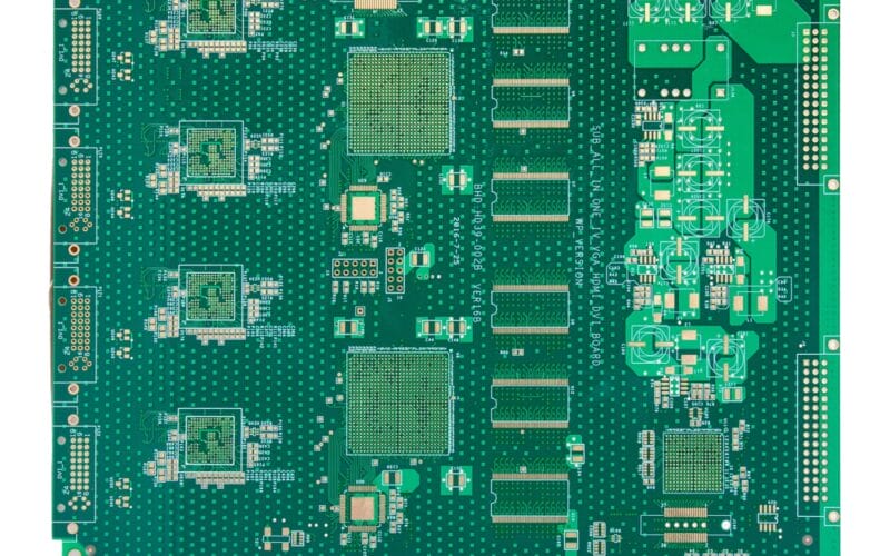
PCB Manufacturing
PCB Specifications
- Layers: 8
- Board Thickness: 1.8mm
- Min. Line Width/Space: 3/3.5 mil
- Min. Hole Size: 0.2mm
- Min. Distance from Hole to Line: 0.13mm
- Inner Layer Copper: Hoz
- Outer Layer Copper: 1oz
- Surface Finish: Immersion Gold
The final board met all mechanical and electrical tolerances and passed electrical testing with 100% yield. This project shows our capabilities to handle complex, high-density multilayer PCBs with tight tolerances and strict quality standards.
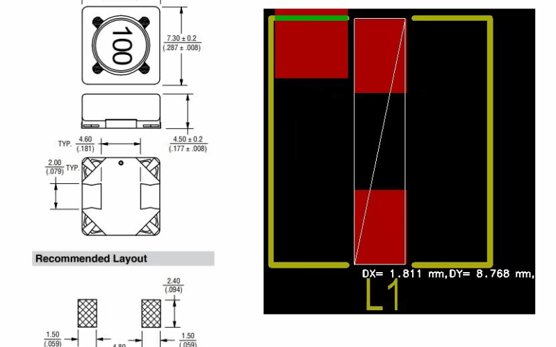
PCB Assembly
Project Details
- Service Type: PCB Assembly
- Location: Italy
- Client Type: PCB Design Company
- Total Units: 20
- Lead Time: Rapid turnaround for prototyping
- Assembly Type: SMT+THT mixture assembly
Our experienced production team worked closely with the client to verify the BOM, optimize the stencil and the board’s layout design. We completed and delivered 20 fully assembled units within the expected lead time, allowing the client to avoid delays and meet their customers’ delivery window. This case highlights our capabilities to support global clients with flexible, low-volume PCB assembly solutions.
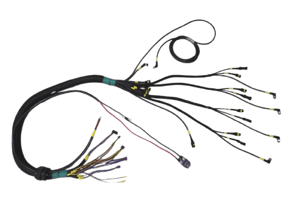
Wire Harness
Project Details
- Service Type: Custom Automotive Wire Harness
- Location: New York, USA
- Client Type: Auto Repair Shop
- Quantity: 10,000 Units
Our team followed strict quality guidelines throughout production, using automotive-grade connectors and insulation materials. The order was completed on schedule with no reported defects, supporting the client’s rollout without interruption. This case shows our comprehensive capabilities in large-scale production, customized solutions, quality control and efficient delivery.
PCB Assembly Services Client Feedback
As an R&D manager, I have had an outstanding experience working with WELL-PCB. For many years, our company has entrusted them with the production, assembly, and programming of the boards developed in our R&D unit, and they have consistently exceeded our expectations.
Hamid Reza Moshayedi
R&D Manager
Their work is very impressively perfect. Today, when they check our company PCB board after assemble. They found a fake short point which many engineers has never found in the past years. But that is just designed so. The PCB board quality is excellent. Their service is also excellent.
MikeZ
My friend introduced WellPCB to me, the first try, a little look forward to. I ordered a 47*72 10ps PCB, and I can’t wait to receive my PCB. So I used expedited service and received my PCB in three days. I tested and soldered the PCB, Quality is really good, silkscreen, plating also great.
Warren Cliton
Assembly Services FAQs
Can you do PCB assembly if I provide my own bare PCB board or components?
If you’d like to source a bare board or components yourself, we’re happy to provide PCB assembly services.
What is turnkey PCB assembly?
Turnkey PCB assembly is an extensive, all-inclusive service model where we handle every aspect of the PCBA creation process. This includes sourcing components, PCB fabrication, and assembly.
Do you offer bulk discounts?
Yes, we offer discounts for large orders. Contact us today to discuss a bulk discount on your next project.
What does your quoted price include?
Your quoted price includes setup fees, stencil fees, assembly service costs, labor costs, components, and shipping.
Ready to Bring Your Electronic Project to Life with Expert PCB Assembly?
Get an instant quote or consult with our experts today. First-time customers get $100 off their order!


