Have you ever thought about how you can take such amazing pictures with your smartphone? Handheld cameras contain CMOS sensors, which are an integral part of making high-quality images. Would you like to find out more about these sensors and their PCB layout? In that case, you’ve come to the right place! Please keep reading to learn everything you need to know about CMOS sensors and discover the guidelines to follow to deliver consistent performance.
Contents
- 1 What Are CMOS Sensors?
- 2 What Is the Difference Between CCD and CMOS Sensors?
- 3 The Importance of CMOS Sensors’ Integrated Nature
- 4
- 5 CMOS Sensor– Other Considerations of CMOS Sensor Layouts
- 6 CMOS Sensor– Balancing Between a Mathematical Layout and Mechanical Enclosure
- 7 CMOS Sensor–Component Placement Guide in High-Speed Layouts
- 8 CMOS Sensor– How to Route High-Speed PCB Circuitry Properly
- 9 Conclusion
What Are CMOS Sensors?
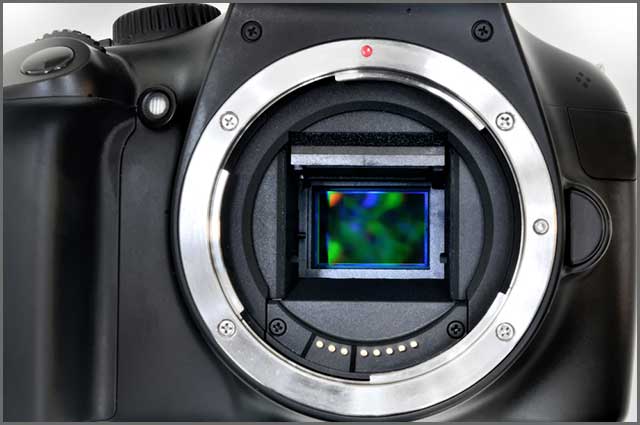
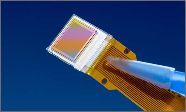
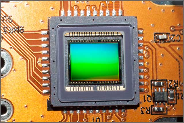
CMOS sensor is a complementary meta-oxide-semiconductor device. It is an image sensor that identifies and transfers information a camera needs to create an image. The sensor detects the light that goes through or hits objects and captures it. The sun gets converted to signals that will later deliver the vision.
The two main types of image sensors are CMOS and CCD. Numerous industries take advantage of these sensors, including consumer electronics, medical equipment, thermal imaging devices used in the hunting and military industry, sonar and radar products, etc.
What Is the Difference Between CCD and CMOS Sensors?
If we are talking about smartphones, digital cameras, and other products designed for individual use, the chances are the sensors utilize CMOS technology. The reason why manufacturers choose them is their affordable price and moderate power consumption. Those are both important for smartphone owners looking to get the best possible battery duration at a budget-friendly price. CMOS sensors are also the primary choice anywhere where you still need photography.
The similarity between CMOS and CCD technology is that they aim to capture light and then transfer it to electrical signals. The specific of a CCD device is that each cell is analog. Upon detecting the sun, a small charge in each sensor holds it in the chip. The nearest amplifier has the task of amplifying the charges in pixels. The process continues until all pixel lines have expanded cost and output.
Unlike that, CMOS sensors have amplifiers for every individual pixel. That means they have a smaller space for capturing the light. It is not an issue because each photodiode has micro-lenses in front of it. Those lenses have the task of focusing the light into the diode. That secures the detection of views; otherwise, you may miss it.
Are you wondering about the advantages of CMOS sensors?
For starters, they don’t have to use as many components as CCD technology. That makes them more affordable and accessible to use in consumer products. These sensors can also be quicker than CCD and have lower power consumption, increasing the battery of your application. Finally, you will also benefit from improved resistance to static electricity discharge.
The Importance of CMOS Sensors’ Integrated Nature
An essential characteristic of CMOS sensors is that they have an integrated nature. Thanks to that, you can include fewer components on your PCB than usual, which can help you to save both space and money.
It is vital to note that these sensors are noise-sensitive. That is crucial to know because they have the capability of delivering low-noise photos. However, you may also deal with noisy or grainy pictures if other components emit EMI or if the supply voltage fluctuates and ripples. All that can cause noise, and you should also be careful of the transient over and undershoot.
CMOS sensors have the task of detecting an analog signal at a pixel level. The next thing they do is converting that signal to a digital number, and that information then goes to an IC in charge of processing external signals. It means that your primary consideration should be ensuring adequate routing of mixed messages.
You will encounter sensors utilizing LVDS and other signaling standards. Make sure that the routing follows the given rule. Another thing to consider is the power supply voltage. You will probably need different sources for the chip’s analog and digital circuits. That is because they utilize a diverse voltage range. While the voltage for digital circuitry may vary, analog has a standard voltage of -3V, although some manufacturers pick a different variety.

CMOS Sensor– Other Considerations of CMOS Sensor Layouts
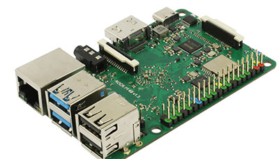
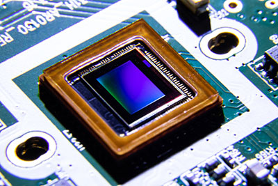
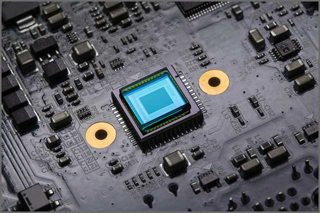
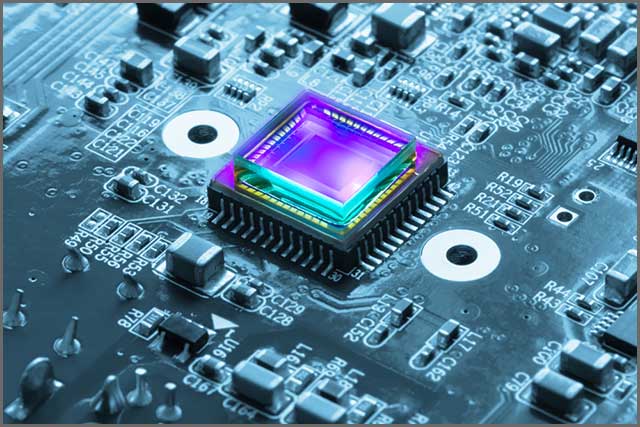
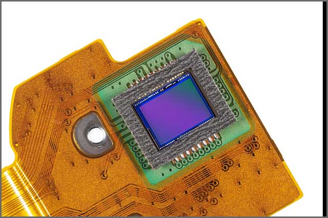
When it comes to mounting CMOS sensors, you will usually use a through-hole or surface mount. In some cases, these sensors might be in the form of a die that you can mount to a BGA package. However, you can also integrate other sensors with the signal processing block. The single SoC (system-on-chip) approach requires four or more layers to keep in mind during stack-up management.
You should use that layer number to set a ground layer below the surface one with the CMOS sensor. The ground plane must have different areas for digital and analog sections. It might not be wise to go with a ground plane split since you may encounter issues with noise sensitivity. You also don’t want any circuits with a high frequency or high speed near the sensor, so consider placing them far away from it.
You can consider using a flex ribbon to route output and input connections over it.
However, you can only facilitate that with the adequate placement of the CMOS sensor on your board. You will also need to consider establishing reliable return paths. Thanks to that, you will decrease the EMI vulnerability of the circuitry, which can be vital to improving the reliability of the sensor and the board. The majority of manufacturers will avoid using a flexible printed circuit board with a CMOS sensor.
If you are looking for a company that can handle the design and assembly of PCBs with an imaging sensor, feel free to contact WellPCB. The project’s complexity is irrelevant because it has years of experience and hundreds of successful projects in its portfolio.
WellPCB can help you throughout the entire process. The knowledgeable staff will assist in making the right decisions for the design of your board and handle the assembly. In the shortest possible timeframe, you will have a top-performing PCB at your doorstep.
CMOS Sensor– Balancing Between a Mathematical Layout and Mechanical Enclosure
It is only natural that the layout of a printed circuit board has certain specifics. For example, it is vital to ensure optimal balance between the mechanical enclosure of your application and the electrical layout. You will need to accommodate filters, lenses, and other optics mechanically and integrate a board that contains the imaging sensor.
Some cameras may also have the possibility to move the optics to set the desired focus. However, printed circuit boards with sensors need to be kept in the same position, even if possible. There are ways to move them, too, but they require advanced geometry.
Fortunately, smartphones have algorithms that allow autofocus these days. It is why you do not have to worry about moving lenses. But you will need to work with both electrical and mechanical teams to secure that everything fits perfectly.
CMOS Sensor–Component Placement Guide in High-Speed Layouts
You will still follow the usual rules for designing a PCB layout. That means you should utilize the DFM (design for manufacturing) approach and create a board that a real-life machine has assembling capabilities. However, a high-speed layout will require some specific considerations regarding component placement.
Circuit paths need to be prioritized because you want the distance that the signals have to cross to be minimal. The pins need to have the most direct possible connection in critical nets, which you need to consider while following the schematic of the circuitry.
You also don’t want the traces of signals to go through split planes. That will secure a reliable return path, which is essential for a high-speed layout. Additionally, consider extra cooling options because you don’t want high-temperature issues if certain parts get too hot.

CMOS Sensor– How to Route High-Speed PCB Circuitry Properly
You shouldn’t expect many surprises in terms of trace routing. However, the trace length requirements may vary, and it is essential to follow the recommended guidelines. If you use the right software or hire an expert, determining the ideal trace widths shouldn’t be a problem.
It is vital to note that the most direct path might not be the best routing solution for your application. Your primary consideration should be to secure high-speed trace routing, and the best way to do that is to consider the complete signal path.
Conclusion
CMOS sensors are beneficial components that secure top-quality images and are an excellent choice for smartphones and other consumer products.
The printed circuit boards that consider these sensors have specific characteristics, and that is something to keep in mind during the design and the manufacturing process. If you want a reliable PCB with a high-performance imaging sensor, you should work with industry experts. Because they can provide a board with sufficient reliability and durability and make sure everything is working.