Contents
- 1 BGA Soldering – Preparation Before Soldering
- 2 Thoroughly Clean the PCB
- 3 BGA Preparation for BGA Soldering
- 4 BGA soldering, Reflow Technology soldering
- 5 Control the Solder of BGA Soldering
- 6 Inspection of BGA
- 7 Align the BGA to the PCB Pad Accurately
- 8 Best BGA solder Joint Standard
- 9 BGA Rework
- 10 BGA Rework
BGA Soldering – Preparation Before Soldering
BGA soldering The first step is picking up a proper surface finish. The finish has to compatible with an upcoming project or the requirements of a product. While there are many available surface finishes, some of them may call for lead-free surfaces. They include RoHS, lead-free OSP, or lead-free ENIG rule.
After picking the right material for your project, you need to ensure that you store the PCBs in the right way. Poor handling and storage may end up ruining your PCBs.
It is thus advisable to store them in a container with a moisture barrier. The case should contain a moisture-sensitive card to alert you of the humidity in the bag. With the moisture-sensitive card, you’ll be able to know about the humidity levels required.
Once you have everything under control, you can now move to the second step.

Thoroughly Clean the PCB
Now that your boards are in the right condition and ready for BGA soldering, you need to ensure that the PCBs are thoroughly cleaned or baked. Baking ensures the eradication of moisture that might later lead to soldering defects. Therefore, you need to ensure thorough cleaning of PCBs before undertaking the assembly process.
With dirty PCBs, you risk encountering BGA solder ball defects. They include cold welding, displacement, voids, and bridging. During storage and movement, your PCBs may end up covered with some dirt. To ensure that thing goes as planned, make sure that your boards are clean before the assembly begins. In most cases, many assemblers rely on ultrasonic cleaners.

BGA Preparation for BGA Soldering
Since BGAs are moisture-sensitive in a way, you need to ensure that you keep them in a dry environment. Those in charge of handling them must conform to the rigorous operations required to keep the components from damage. In general, though, these components should be kept inside moisture buster cabinets. The temperatures should range between 20℃ to 25℃ and a humidity of approximately 10%.
As noted earlier, there’s a need to bake BGA components before starting the soldering process. Here, manufacturers need to ensure that the soldering temperature doesn’t exceed 125℃. Otherwise, it may bring about an undesirable metallographic structure. Again, caution is essential here since if the temperature is low, it becomes hard to get rid of moisture.
So, it’s essential to bake components before undertaking the SMT assembly. It ensures the elimination of moisture inside the BGA. Additionally, BGAs need about 30 minutes of cooling after baking and before entering the SMT assembly line.

BGA soldering, Reflow Technology soldering
Typically, the assembly package of BGA is the same as the SMT assembly. First, solder paste gets printed on a pad array of a PCB by applying stencil or flux onto the pad. Secondly, you introduce the pick-and-place equipment to align BGA components on the PCB. After that, subject the BGA components through a reflow soldering oven. Reflow technology soldering is a complicated process that involves a couple of phases, as briefly highlighted below:
1. Preheating phase –this phase is usually composed of 2 to 4 zones of heating. Here, the temperatures can go as high as 150℃ in under 2 minutes. For this reason, there are no instances of solder splashing or an overheated base.
2. Soaking phase – here, the target is to achieve hot melting, something that makes good soldering joints.
3. Soldering phase –this phase needs to witness the temperature of solder joints rising to that of the soldering temperature. Here, it’s best to set high temperatures so that the joints come out as desired.
4. Cooling phase –this is the last step of reflow technology soldering. It contains two modes of cooling: natural cooling and air cooling. It’s ideal for the cooling rate to be between 1 ℃ and 3℃.
Control the Solder of BGA Soldering
The fifth step is to ensure that you control the solder during the BGA soldering. On most occasions, when soldering, the temperature surpasses the melting point, with the solder getting melted to become liquid.
But to ensure that everything comes out as desired, you must control the solder of BGA soldering. You achieve this by maintaining temperature levels of about 183 degrees for 60 to 90 seconds. Either too long time or too short time frames may cause quality issues when undertaking BGA soldering. Sometimes, you may have to check your soldering knob. A majority of them have a knob when turned, reduces the heat of the iron. It thereby controls the solder and lets you have the desired results.


Inspection of BGA
Before releasing your products to the market, ensure that the BGA soldering undergoes a thorough inspection. Without inspecting your products, there are chances that you’ll produce faulty products. These products may need a costly rework, ruining the reputation of your business. The same is true when it comes to BGA inspection. In PCB assembly, BGA inspection is one area that has brought a considerable amount of interest since the introduction of BGAs.
It should be clear that you cannot effectively carry out BGA inspection by using optical techniques. The solder joints underneath the BGA components aren’t visible. Additionally, it’s not easy to test the solder joints by checking for electrical performance.
The only satisfactory way of testing BGA is by using X-rays. X-rays have proved quite helpful in identifying the solder the joints located underneath the package. They are thereby assisting in a detailed inspection.
But X-ray is not the only method that one can use. Even though X-ray comes in as one of the most effective methods, designers still have other options. They may choose to use boundary scan or electrical testing to check for BGA welding quality. For instance, electrical testing only reveals electrical conductivity. On the other hand, it fails to check for the success of BGA soldering.

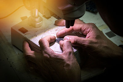
Align the BGA to the PCB Pad Accurately
The seventh step involves the alignment of the BGA to the PCB pad correctly. There are two stages involved here. The initial alignment, followed by maintaining alignment during the process of soldering. To achieve this, you need special equipment for mass operations. However, if you need to create a prototype, you can still manually align. It is also known as manual alignment.
To ensure that everything comes out correctly, you have to mark the boards effectively with some alignment marks. These marks are preferably made of copper. Also, you need to avoid using solder paste as it may melt during muscular surface tensions. It causes damage to the terminals in the long run.
Again, if you are running high-volume production, it may be time and cost-saving if you consider optical alignment. You need to also invest in specialized machines with the ability to align everything on the PCB pad.

Best BGA solder Joint Standard
There are specific BGA solder joint standards that you must adhere to if you want to undertake BGA soldering on PCBs during SMT assembly. For instance, BGA soldering joints that have cavities in them lead to many failures. They are also likely to have other costly technical issues in the long run.
For instance, according to IPC BGA soldering standards, if it is challenging to avoid cavities on the pad, such holes shouldn’t be 10% larger than the solder ball area. In other words, the tunnels on the pads must not be larger than 30% compared to the solder ball’s diameter. To ensure good results, you may have to stick to acceptable industry standards regarding BGA solder joints.

BGA Rework
As you may be aware, it’s a bit tasking to undertake BGA rework. But it eases if you have specialized equipment at your disposal. But, if you have to return your product(s) for repair, then there’s no reason to worry as such. Repair work begins by first heating the BGA components. It ensures that you melt the parts underneath.
A particular rework station is ideal during rework. It is also perfect for a tasking process comprising specialized equipment such as an infrared heater, a vacuum device, and a thermocouple monitor. Here, great care is necessary to ensure the removal of BGA components only. A slight mistake may damage the entire board.


