
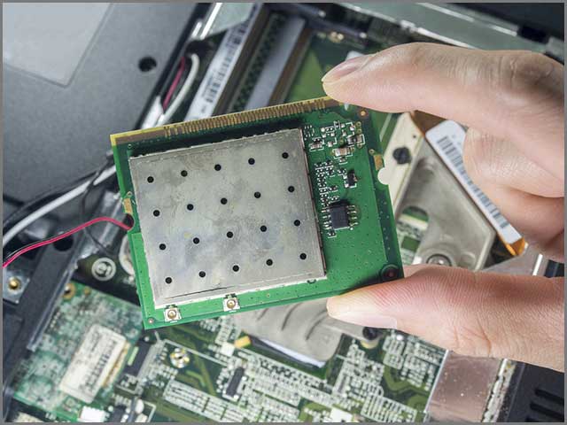
HDI PCB Layout is not easy, considering the many factors that go into coupled with the complexity of the designing process itself. This level of difficulty goes up a few notches when you want it customized to meet your specifications. Your best bet is to find the right manufacturer to manufacturing an HDI PCB that’s just right for your business needs.
That said, you should also know the specific aspects that go into the design so you can see the customization aspects, and based on it, you can choose the right manufacturer to make this custom design for you.
Contents
Aperture Ratio
One of the first things to consider in a hole design is the aperture ratio. If you’re planning to use the traditional mechanical drilling process, your hole aperture should be no more than 0.15mm, and the rate of board thickness to aperture should be 8:1. You can go up to 12:1 in particular circumstances, but it is best to keep it at the usual 8:1 ratio.
In laser drilling, the aperture of the drilling hole should be 3 to 6 millimeters, though four is the most ideal. Also, the hole depth to aperture should be in the ratio of 1:1.
It’s important to note that the aperture size gets smaller during the plating process when the board thickness increases because it’s difficult for the chemical solution to penetrate through very thick boards. Also, when the voltage rises, the defects become more visible, resulting in a complete failure of the board.
To avoid these problems, ensure that the PCB designing company you choose is familiar with these ratios and techniques. Otherwise, you’ll end up with a high scrap rate and possibly even a failure in fabrication.

HDI PCB Stack up Types
The classification basis of HDI PCB Stack up is the order of layers with blind holes. Let’s take a look at some of the popular categories.
2.1. 1-HDI
In this category, the structure of buried and blind holes is in this order.
- 1-2 is a blind hole
- 6-5 is a blind hole
- 2-5 is a buried hole
2.2. Non-stacked 2-HDI
The structure of a non-stacked 2-HDI is as follows.
- 1-2 is a blind hole that is not stacked
- 2-3 is a non-stacked blind hole
- 8-7 is a non-stacked blind hole
- 7-6 is a non-stacked blind hole
- 3-6 is a buried hole
2.3. Stacked 2-HDI
Here is how a stacked 2-HDI type looks like.
- 1-2 is a stacked blind hole
- 2-3 is a stacked blind hole
- 8-7 is a stacked blind hole
- 7-6 is a stacked blind hole
- 3-6 is a buried hole.
2.4. Stacked and resin-filled 2-HDI
In this example, this is how the ordering of layers is as follows.
- 1-2 is a stacked blind hole
- 2-3 is a stacked and resin-filled blind hole
- 8-7 is a stacked blind hole
- 7-6 is a stacked and resin-filled blind hole
- 3-6 is a buried hole.
These examples bring out the need for designers to consider the right asymmetric design to ensure that the distribution of buried and blind holes is so that the yield from the board is maximum. If there is no uniformity in the structure of these holes, it can lead to stress and the formation of one-sided warpage, all of which can eventually decrease the board’s yield.
HDI-PCB Design Process Flow
The process flow is essential for any design, and an HDI-PCB, in particular. There is a specific way to drill holes to ensure that the board is stable and gives a good yield, and you should find manufacturers who are aware of the exact process for the design.
Let us take the example of two types of stacking to get an idea of the process flow and its overall importance to the design.
3.1. 4-layer HDI with one stacking
In general, the process flow for a 4-layer HDI is relatively similar to that of an ordinary PCB. The only difference between the two comes in the sequence of drilling holes. Designers and engineers have to start with buried holes of 2-3 layers, followed by the mechanical drilling of 1-4 layers, and finally, the blind hole of 1-2 and 4-3.
If this process is not followed, it can cause extreme fabrication problems, thereby increasing the cost of scrap and production.
3.2. 6-layer HDI with two stacking
In this case, the process begins with the drilling of buried holes in 3-4 layers followed by 2-5 layers, blind holes on 2-3 and 5-4 layers, holes on 1-6, and finally, the drilling of 1-2 and 6-5 blind holes.
Despite such a rigorous process flow, 6-layer HDI with two stacking is not recommended except for advanced products. The product scrap rate will be high, and accumulated counterpoint errors cannot be eliminated.

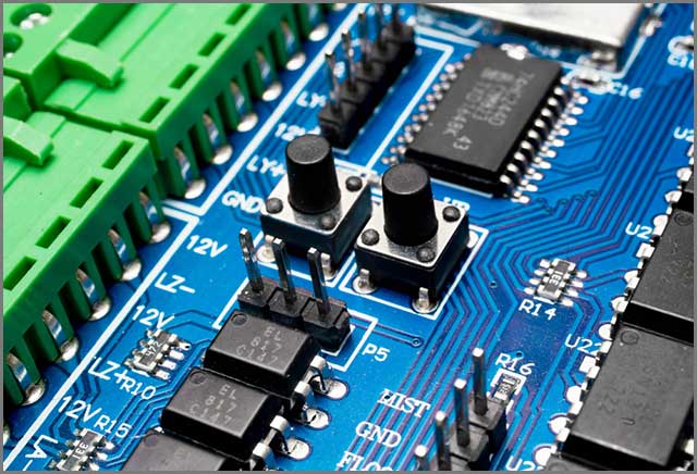
HDI-PCB Layout of components
Another essential aspect to consider while designing HDI-PCB boards is the layout of components. The spacing between components has a big impact on the solderability and maintainability of the boards.
Ideally, the manufacturer you choose should adhere to the following spacing to avoid problems during installation.
- Ordinary SOP and PIN of other components should have a minimum distance of 40 millimeters between each.
- BGA and PIN of other components should be at a minimum distance of 80 millimeters.
- A PIN in ordinary components can have a spacing of around 20 millimeters.
- RF, analog, and digital parts must be separate in terms of space. Also, there should be high spacing among them, regardless of whether they are on the same or different side.
- High power signals should be far away from other signals.
These are minimum specifications, and the manufacturer should strive to give as much gap as possible to make it easy to solder, assemble, and do any rework if necessary.
As you can see, the layout has a significant bearing on your board’s design and final performance.

Tracking
A reliable manufacturer should consider many different aspects in tracking to ensure that the final design is stable and as per your needs and expectations.
Some of these aspects are:
- Components on the top and bottom layers should have good isolation. on
- Mutual crosstalk between the inner layer signals should be at a minimum level.
- For RF signals and analog areas, ensure that there is a right reflow path around each sign.
- Track necessary signals with high impedance levels at a more top priority than other signals.
Following these tracking considerations is necessary to avoid short circuits, open circuits, weak absorption, and other problems plaguing poor design.

HDI PCB Layout–Pad Size
Pad size has a big bearing on the design outcome, especially in size and weight. It can also reduce the overall size of the electronic product if that is one of your design goals.
Below are some ideal pad sizes, though customization of these sizes is possible based on specific requirements.
- The pad size should be three millimeters over drill size for Blind Via and 10 millimeters over drill size for Buried Via and Through Hole, respectively.
- Advanced option, the pad size should be six millimeters over drill size for Blind Via and 14 millimeters over drill size for Buried Via and Through Hole, respectively.
- For standard boards, the pad size should be eight millimeters over drill size for Blind Via and 20 millimeters over drill size for Buried Via and Through Hole, respectively.
HDI PCB Layout–Material
PCB contains four layers, all of which are heat laminated into a single layer. The materials used from the top layer to the bottom include Silkscreen, solder mask, copper, and substrate. Out of these, the substrate layer is fiberglass and is often called FR4, which denotes fire-resistant. The thickness of this substrate layer can vary according to the requirements and the device.
There are many sub-categories in each of the above four layers that can depend on your requirements.
Though they are the standard ones, boards made of cheaper materials are also available. But these boards don’t last for a long time and tend to lose their lamination quickly, depending on the material used. You can even identify these cheap materials by the smell they give out during the soldering process.
The onus is on you to find a manufacturer who will use the best materials for your requirements.
HDI PCB Layout–Conclusion
We hope this information gives you a general idea of your aspects while designing an HDI PCB. If you plan to find a manufacturer to do this job for you, make sure the company you choose understands these aspects in-depth and has the experience and skill to create the right board for your needs.
The right manufacturer will know these things by heart and not expect you to input these special considerations.


