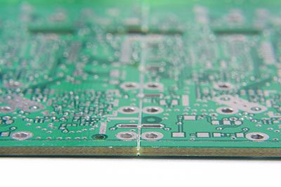
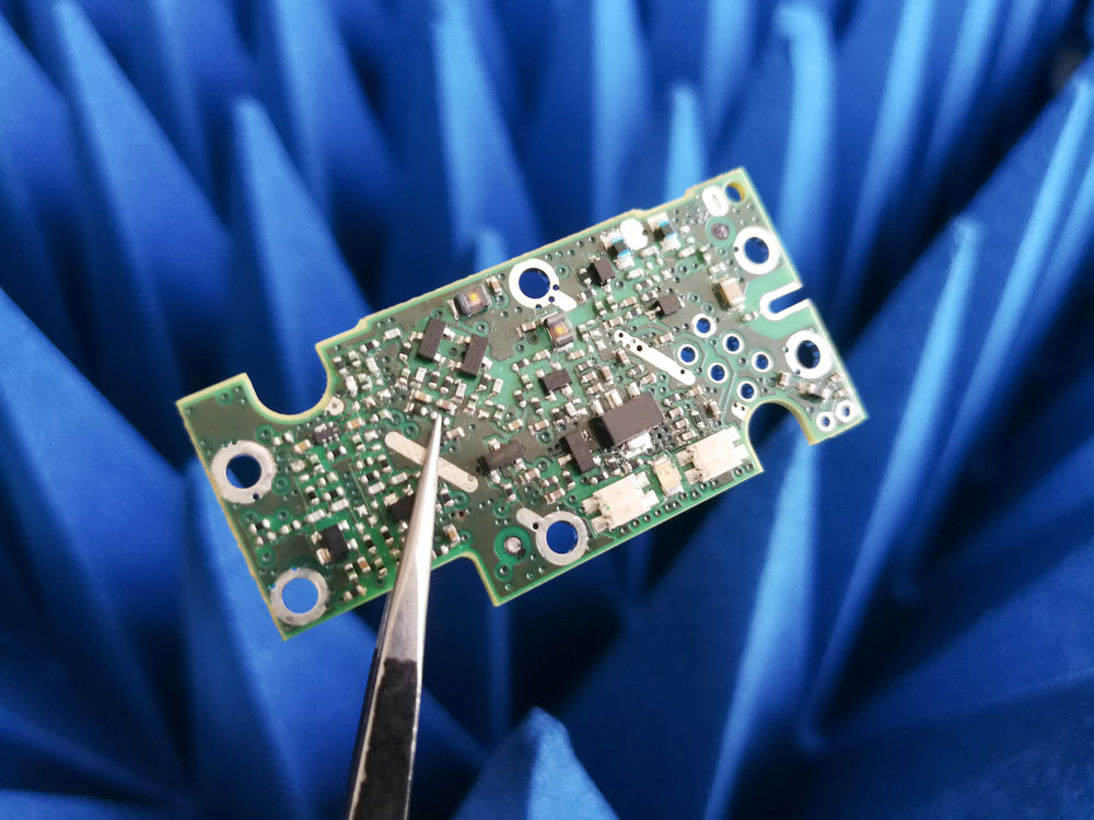
AOI Inspection stands for Automated Optical Inspection systems, mainly used for PCB manufacturing, bare board inspection, board assembly, board rework, and assembled board inspection.
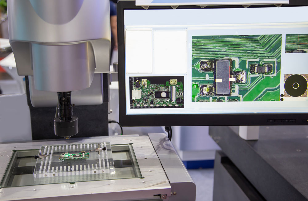
The contactless assessment method of PCBs is highly efficient for improvement in process quality. In AOI, an autonomous camera scans the board continuously.
A generic CCD camera, IR camera, or microscope is mounted with zoom capabilities.
The AOI Inspection is used in all stages of PCB assembling, from paste printing, components placement, reflow soldering, and post-soldering components inspection.
True viewing:

Contents
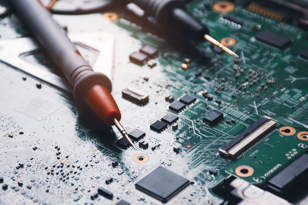
A PCB is inspected during and after manufacturing. For example, after manufacturing, the ET (Electrical Test) test ensures no short-circuiting between two different nets or tracks.
It is an error of UV exposure or the etching process where a small hair-like copper remains unexposed to the UV light and cannot be removed during the etching process.
Post-manufacturing PCB inspection with AOI includes:
1. Line or track width violations:
The track should be within a specific width range specified by the designer. Over-etching makes thin tracks and removes extra copper.
Under-etching makes wider and short-circuited tracks because unnecessary copper is not etched or removed.
2. AOI Inspection—Excessive copper:
Copper is not etched from large areas of copper over PCBs, and tiny dots of copper remain intact.
3. AOI Inspection—Missing Pad:
Paste of insufficient etch-protective layer keeps the pads or vias uncovered and obliterates it during the etching process.
4. Clearance Violation:
Clearance violation is most of the time by the designer. However, insufficient etching makes a smaller clearance than required.

5. AOI Inspection—Sort circuit:
A short circuit appears in the PCBs like a minimal and thin trace connecting two tracks/pads and vias. This type of short circuit is not visible to the naked eye, especially in the inner layers of the multilayer PCBs. For this purpose, a high-resolution microscope or X-ray scope is used.
6. Copper Cuts:
Copper cuts are generally found in PCBs, mainly due to scratches on the PCB sheet. This fault is also a fragile hair-like structure that cannot be resolved with the naked eye.
7. Scratched or Hole Breakage:
In the electrolysis process, the holes are not formed properly and have broken from inside the recess, forming the annular ring, or the pads are ripped off.
8. Silkscreen placed over pads:
The component’s information, like designators, assembly marks, PCB names and notes, and identification marks, are placed over the solderable areas like pads.
It makes an inferior soldering joint between the pads and pins of the components.
9. Solder Bridging:
AOI is also used for post-assembly and soldering inspection of the PCBs for solder bridging or short-circuiting due to extra solders over two nearby pins.
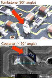
Fig. 1:- Assembled PCB components placement and soldering inspection by AO machines