A CNC drill machine with many drill heads can drill all the different hole sizes needed at a high rate. Devices differ by speed, PCB Drill Sizes, and x-ray optimization.
When a PCB is made, there are a couple of things to keep in mind related to drilling: the size of the holes and the type of hole.

Contents
PCB Drill Sizes–Content

As it relates to hole size, consider the aspect ratio relative to the manufacture of the PCB. Aspect ratio is the ratio between the board’s thickness and the drilled hole’s size before plating. It is used as a guide to ensure that a manufacturer does not exceed the mechanical capability of the drilling equipment or the available drill sizes.
Some standard material thicknesses and corresponding PCB drill sizes:
0.031″ Thick – Smallest Hole 0.006″ (smallest BAC can do mechanically)
0.062″ Thick – Smallest Hole 0.006″
0.093″ Thick – Smallest Hole 0.009″
0.125″ Thick – Smallest Hole 0.012″
Use the “preferred minimum hole size” on their PCB board designing company website.
In practice, there is a balance between:
1.If you make the vias too big, they require lots of space on your PCB (on every layer), making it more difficult to route and perhaps requiring a bigger, more expensive PCB.
2. If you make the vias a little too small (less than the “preferred minimum hole size” of a particular manufacturer), then that specific manufacturer will claim it requires a “special process,” which adds expense.

3. If you make the vias much too small (less than the “absolute minimum hole size” of a particular manufacturer), then that manufacturer can’t make it at all, and you’ll be forced to find a different (probably more expensive) manufacturer or redesign the board.
A via’s “metal barrel” is practically free if you have any plated through holes. The PCB fab throws the PCB in the through-hole-plating bath until an appropriate thickness of metal grows in every hole.
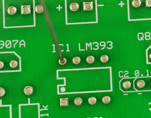
Fig.(3)
Many manufacturers publish their “standard hole sizes” (standard drill bit sizes minus the standard barrel thickness of through-hole metal plating).
The man running the drill press prefers to see standard sizes; otherwise, he is forced to either (a) pick the next smaller standard drill bit — then the physical part won’t fit in the hole; (b) pick the next larger drill bit — this pushes the through-hole metal plating out, possibly hitting some internal trace and rendering the entire board unusable; or (c) reject the board as manufacturable.
To avoid all three problems, PCB designers often “round up” non-standard hole sizes to the next larger standard hole size — i.e., holes for DIP packages are usually rounded up to 0.9 mm diameter — and then run the DRC check.
If the DRC finds any traces that are now “too close” to the giant hole, the designer pushes those traces a safe distance away before sending the design to the manufacturer.

How to Calculate PCB Drill Size
Knowing the correct PCB drill sizes is typically a cost-determining step. It makes the difference between using existing drills or making custom drills.
The drill sizes of the PCB have to match a certain PCB drill size to board thickness ratio. That being said, let’s see how manufacturers calculate PCB drill sizes.
Establish Components’ Lead Diameter
Let’s assume you have all your PCB electrical components. Each component has a standard diameter. You’ll need to check all the components’ lead diameters.
Then, arrange the components, starting with the thickest lead diameter.
Usually, the packaging or the datasheets have diameter labeling on them.
For example, you can expect a 1.2-1.5mm diameter from terminal blockers and trimmers.
Components such as ICs and resistors have an average diameter of 0.8mm, while D and IDC connectors have a 1.2-1.5 diameter range. The same case applies to larger diodes.
Determine Minimum Hole Size
It’s not enough to know just the diameter size. You must know the hole sizes to go with the diameter.
Take the maximum lead size in the previous step.
Apply the following equation to determine the minimum hole size.
“0.25mm + the Maximum Lead Diameter”
Find the Pad Diameter
Finding the accurate pad diameter requires an accurate minimum hole size. That way, you can use the smallest pad area.
You will likely end up with a 0.55 mm or 50-micrometer pad diameter. Furthermore, include a margin for fabrication allowance.
With all these numbers in the record, follow this formula to find the pad diameter.
Minimum Annular Ring x 2 + Minimum Hole Size + Minimum Fabrication Allowance
Decide The Density Level Difference
There are three levels of component density during the PCB-creating process.
Most manufacturers would prefer Level A density. It has a low component density that guarantees near-perfect footprint geometrics.
However, level B is a great hack for manufacturers since they can get dips, waves, reflows and drag soldering. They’ll go for Level B density to ensure solder attachments are secure.
The last level density, C Level, is common in portable device PCB manufacturing.
A skilled manufacturer will attain high design productivity and component density.
Finally, C Level density leaves smaller footprints.