Contents
What are QFN Packages?
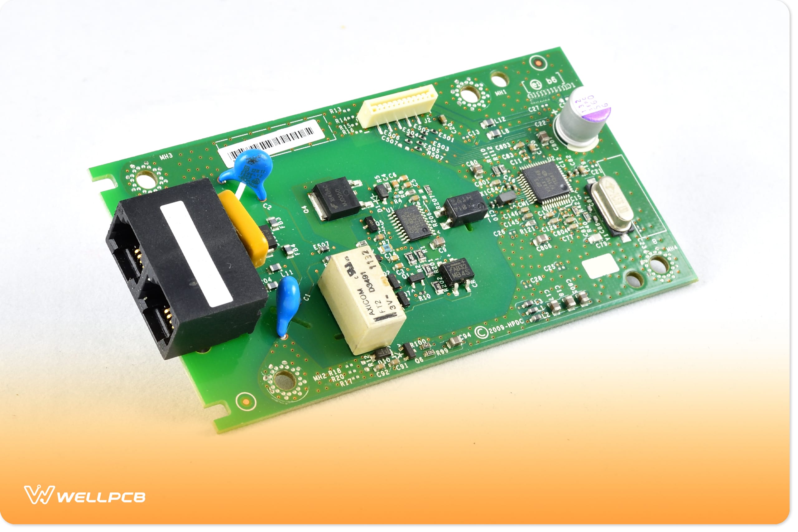
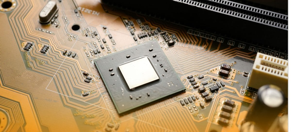
QFN is a semiconductor package that connects the ASCIC to a PCB. And it does this by using surface-mount technology.
Further, the QFN is a lead framed-based package called a Chip Scale Package (CSP). And it’s because it allows you to see and contact leads after assembly.
Typically, a copper lead frame makes up the QFN packages’ PCB interconnection and die assembly. Plus, this package can either have a single or multiple rows of pins.
That said, the packages’ single-row structure forms by a saw singulation or punch singulation process. Both procedures split an extensive collection of packages into single packages.
Furthermore, the multi-row QFN undergoes a copper etching process to get the preferred number of pins and rows. Then, a saw will cingulate the rows and pins.
Also, QFNs usually have an opened thermal pad beneath the package. Hence, you can solder the packet directly to the PCB if you want optimum heat transfer from the die.
Types of QFN Packages
There are different types of QFN packages. Here are some of them:
Plastic-Molded QFNs
Interestingly, this package is pretty cheap. The plastic-molded QFN doesn’t have a lid, and it has two parts: a copper lead frame and a plastic compound. But it’s limited to applications that have about 2 – 3 GHz.
Air-Cavity QFN
This QFN features an air cavity in its package. It consists of three parts: a plastic or ceramic lid, copper lead frame, and plastic-molded body (without seal and opened). Also, this type of QFN is pricey because of its construction. But you can use it for microwave applications ranging from 20 to 25 GHz.
QFN with Wettable Flanks
The QFN with wettable flanks features an elevation that indicates solder wetting. Hence, it’s easy for a designer to visually check and make sure the pads mount on the PCB.
Punch-Type QFN
This type of QFN has its package molded in a single mold cavity format. A punch tool separates the mold cavity, hence the name. Also, it means that you can only get a single package molded with this method.
Sawn-Type QFN
This package involves using MAP (mold array process) for molding. The procedure entails cutting a massive set of boxes into smaller parts. Then, you can finalize the process by sorting the sawn-type packages individually.
Flip Chip QFN
The flip-chip is a cheap molded package. The box uses flip-chip interconnections on a substrate (copper lead frame).
Thanks to its short electrical path, it’s the ideal Quad Flat No-Lead for electrical performance.
Wire Bond QFN
This package connects to PCB tracks, semiconductors, or integrated circuits directly with wires to the chip terminals.
QFN Assembly
Here are the basic steps to use for surface-mount assembly of the QFN components:
Step 1 – Do Some Solder-Paste Printing
First off, you have to start the assembly with solder paste printing. The process involves spreading solder paste uniformly on your board before putting the components.
Step 2 – Placement of Components
You can start mounting your QFN IC components on your board based on the layout of your PCB design. Also, it’s vital to use accurate and precise tools in this stage because the components have high interconnection density.
Step 3 – Perform a Pre-Reflow Inspection
This step is vital because you have to confirm that the board is fit to enter the reflow oven. While you’re at it, ensure that your board doesn’t have contaminants on its surface that may alter the soldering process.
Step 4 – Proceed With the Reflow Soldering
Please place it in the reflow oven for soldering once you confirm that your board is in good shape.
Step 5 – Inspect Your Board After the Reflow Soldering
The reason for this step is to confirm the solder quality.
Also, it’s vital to note that you need a stencil design and an appropriate PCB footprint for the assembled components. That way, you’ll work based on the design intent.
How Do You Solder a QFN Package?
As mentioned before, soldering is a crucial part of the QFN assembly process. So, when the PCB enters the reflow oven, some board parts heat up faster than others. And this happens because of the temperature in the reflow oven.
The parts that heat up fast are the lighter parts of the board. However, the areas with large copper areas take a longer time to heat up. That said, you can use thermocouples for the entire process.
This device helps you to monitor the QFN package’s surface temperature. In addition, the thermocouples help you ensure that your peak package body temperature (Tp) doesn’t surpass typical values.
Advantages of QFN Packages
- The package doesn’t have lead co-planarity issues.
- It has a small footprint which helps to save space on PCBs.
- QFN uses regular surface mount equipment and flows for PCB assembly.
- The package is relatively thin, i.e., the QFN has less than 1mm package height.
- It has remarkable thermal performance (considering that it offers an excellent route for heat transfer from the die to the board when soldering).
- The components on the board can be close to the QFN’s components because of the small size, location, and form factor of the contact pads.
- QFN has a slight package lead inductance.
- Excellent electrical performance.
- The semiconductor package is affordable.
Problems with QFN
The QFN is a fantastic package, but it comes with snags like:
Manufacturing Issues
As a PCB designer, one of the significant concerns with the QFN is manufacturability. It may be challenging to have a reduced defect rate in placing and reflowing the QFNs.
No doubt, the QFNs had some success when they entered the low-mix, high-volume products. But the package tends to have potential issues with the high-mix, low volume operations. This issue cuts across two significant areas: board and stencil design.
So, for your stencil design process, you have to be accurate with your aperture design and stencil thickness. For instance, if you have too much voiding or paste, it will affect your stencil design. Hence, the best approach is to stick to the manufacturer’s guidelines. Aim for a solder thickness of about 2 – 3 miles.
Also, your aperture ratio to pad should be about 0.8:1—with many smaller apertures. As for the board design, ensure that your bond pad design is about 0.2 to 0.3mm away from the package footprint.
Soldering Issues
Due to the package’s narrow pad-to-pad pitch, there’s an increased risk of solder-bridging. And the QFN doesn’t have any lead. So, you may have challenges if you have to desolder the package.
Compatibility with Some OEM Processes
The QFN packaging may be prone to dimensional changes at the board or the part. And this usually happens because the package has no lead. Hence, it’s less robust when you expose this IC package to some extensive ranges of some OEM practices or nominal CM.
Also, board flexure is another dimensional change that this package may experience. In other words, if you subject the QFN (flat package) to activities like in-circuit testing, board attachment, etc., the components will be under high stress. And this happens because the package doesn’t have long, flexible copper leads.
What’s the Difference Between QFN and QFP?
The QFP means (quad flat pack). The differences between both arrays of packages include the following:
| QFN | QFP |
| Leads extend on the four sides of the package. | The lead extends out in an L-shape or gull-wing shape. |
| Average footing for the package during the PCB assembly process. | The lead form has an excellent base for the package during PCB assembly. |
| No variants | Some of the variants include very thin QFP (VQFP), low-profile QFP (LQFP), thin QFP (TQFP), etc. |
| The package has only eight pins and a thermal pad. | Has different pins ranging from eight to seventy pins per side. |
Final Words
QFN packaging is the way to go if you want a lightweight option that is easy to handle. Also, this leadless IC package is effective for connecting the IC’s silicon die to the printed circuit board.
In addition, the packages are perfect for applications that need good heat dissipation. And the assembly is a walk in the park. All you need to do is stick to the steps we highlighted in this article.
What do you think about the QFN package? Do you need to get the best one for your next project? Please feel free to reach us.