EasyEDA is a user-friendly PCB design software. However, you may encounter an issue or two, especially if it’s your first time using the tool. We tried to identify some PCB schematic-related problems and offer solutions. Take a look at the list below, and discover a way to solve your problem!
Contents
- 1 What Is EasyEDA?
- 2 Can I Use EasyEDA for Automatic Routing?
- 3 How to Solve the Problem of Multiple Circuits on a Board in EasyEDA?
- 4 How Do I Add or Edit a Footstep for a Component That Misses a Footstep in EasyEDA?
- 5 Connect Pads in EasyEDA
- 6 How Do I Upload Eses EEDYEDA PCB Files to EasyEDA Software? What Steps and Documents Are Needed?
- 7 Comparison of EasyEDA With Other Software
- 8 Summary
What Is EasyEDA?
EasyEDA is a state-of-the-art PCB design tool designed to fit both beginners and experts. If you are a newcomer to the printed circuit board design, you will benefit from the easy interface of the product. The experienced users will appreciate a wide range of useful features that allow them to design their PCB to the smallest detail.
More than a million libraries will help you to create the desired layout of your PCB. The product is available in online and offline variants, which means you can either run an Online Editor or download a desktop client.
Is EasyEDA Free?
EasyEDA offers a free software solution available to all users. That means the editor’s full features are forever free, and you can use it for commercial purposes.
Don’t forget that you also have an option to order your PCB from the website. As soon as you finish your design, you can use Fabrication Output to go to the site and place your order with a registered account. The company offers affordable rates and quick delivery while ensuring that professional staff will take care of all specified instructions.
Can I Use EasyEDA for Automatic Routing?
Automatic routing is an incredibly useful feature that can save a lot of effort when designing printed circuit boards. Software creators recognized that and implemented this tool.
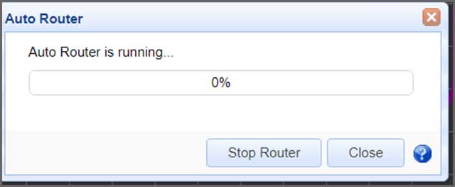
If you want to use the EasyEDA autoroute, start by choosing it from the “Route” submenu at the top of the screen. You will have options to configure the automatic router now.
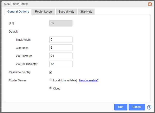
Feel free to adjust things like track width, clearance, router server, etc. Once you run it, you will need a bit of patience to get a completed board. The process might take several minutes.
Please note that you also have the option of using the local auto-router. It is more reliable than the cloud option, and you can download it here.
How to Solve the Problem of Multiple Circuits on a Board in EasyEDA?
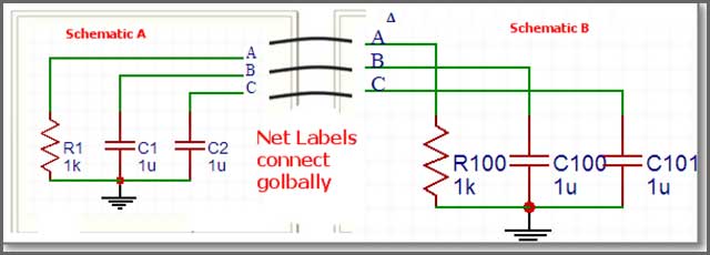
If you are handling a complex project, you may need a multi-sheet design feature. EasyEDA is ready to provide that, which gives you a chance to have multiple schematics within a single project. You can use NetLabels/netPorts to establish connections.
Now, let’s say you use a “DATA0” netlabel in the first sheet. You can use the same in the second sheet because the software utilizes global nets.
Please note that the schematics will be merged during conversion, and the software will connect in netlabel, net flag.
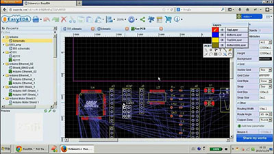
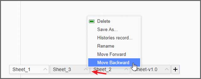
While you are in the Easy EDA PCB design software, you can notice available sheets in the bottom-left part of your screen. Pick a particular tab and hit right-click to delete, rename, or save it, as well as see its historical record. You can also adjust the order of sheets as you wish by selecting moving backward or forward.
Please note that the software utilizes unique global prefixes. You will get an automatic annotation of the prefix when you add it to a sheet. As a result, you will need to confirm unique prefixes when saving a sheet to a different project. You may encounter a prefix conflict issue if both Sheet X and Sheet Z have “R1” annotation.
How Do I Add or Edit a Footstep for a Component That Misses a Footstep in EasyEDA?
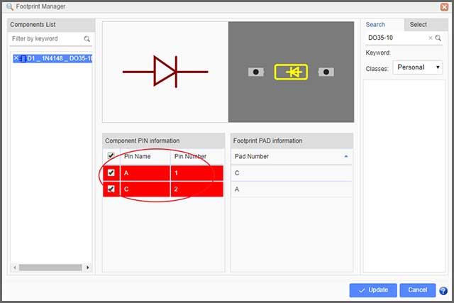
First, you want to open the Footprint Manager. You can do this from the Tools menu at the top of your screen. Now, once you choose a component, check out the custom attributes in the package input box.
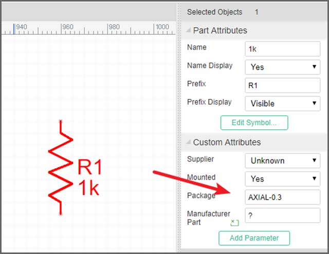
The feature will check whether the package components are correct, and you will get information that something is wrong. That may happen if PINs and pad numbers do not match.
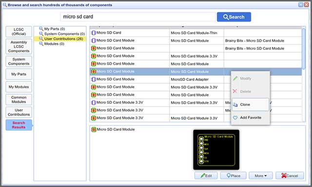
If you want to modify an existing package or footprint, you can use SHIFT + F to find it among the available PCB libs. After you select it, a preview will appear. You want to clone it by using right-click and selecting the Clone function.
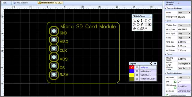
Once you rename the copy, find and edit the renamed file. You can open it with the PCB Lib editor, and make the necessary changes. Don’t forget to save it!
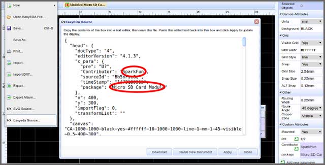
Now, go to the Source Editor of your EasyEDA and use double quotes to enter the new package name, and also change the contributor. If everything is correct, you can save the edit, and it should be available in My Parts.

Connect Pads in EasyEDA
Although it may be more difficult that way, you can design a printed circuit board without using a schematic. In this case, you will need to connect and name pads and tracks manually. The good news is that the Pad-to-Pad connecting feature can make the process easier.
You can use this tool available within the EasyEDA to create a netlist of PCB connectivity when not utilizing a schematic. Please note you can’t draw ratlines between vias and pads that are isolated and don’t belong to a component PCB footprint. You can, however, draw ratlines among PCB footprint pads, regardless of their position.
The Pad-to-Pad Connection tool serves for easier connection of the PCB design. It is only after using this feature that you can start tracking (routing).
Although this tool is useful, wne advise you to go with a schematic whenever you have the option, especially if you are a beginner.
How Do I Upload Eses EEDYEDA PCB Files to EasyEDA Software? What Steps and Documents Are Needed?
Would you like to see how your Online Gerber Viewer. The tool is also free to use, and it allows you to visualize the standard Gerber RS-274X format. Here is a step by step guide that will allow you to upload files to the software.
Step 1: Upload Files
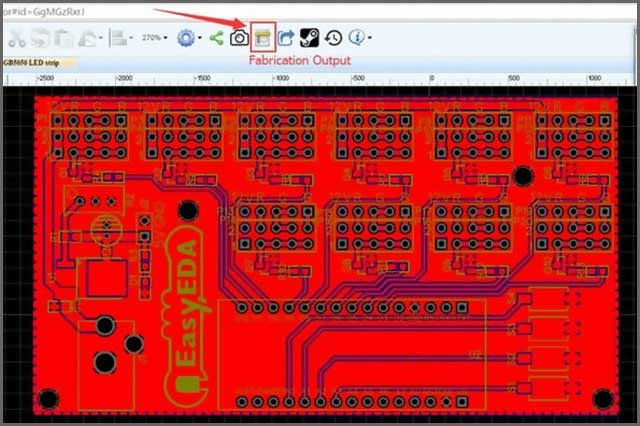
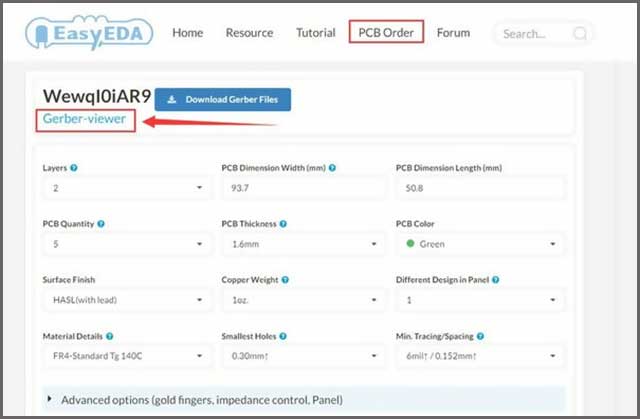
You have the option of seeing your files as images if you go to the online viewer. Alternatively, you can also choose “Fabrication Output” from the top menu on your EasyEDA screen.
The software will take you to the page where you can order the PCB, but you will also have a link to visualize its design.
Step 2: Check Out Your Design
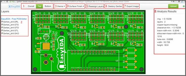
It is easy to use the Gerber Viewer as its interface is beginner-friendly. Thanks to the different options available, it is an excellent way for a newbie to understand different files.
The software allows you to pick surface finish materials, as well as PCB colors from the “Theme” section. You will notice them on a screen in an image form. The tool will even provide a bottom and top image view.
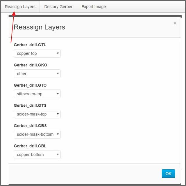
When it comes to modifying, you have the option to show or hide layers in the “Layers” segment. Thanks to that, you can get the exact image you want to see. If you need to make a manual adjustment, you can reassign the layers.
Step 3: Export the Image
If you want to see an actual image of your design, you can always export it.
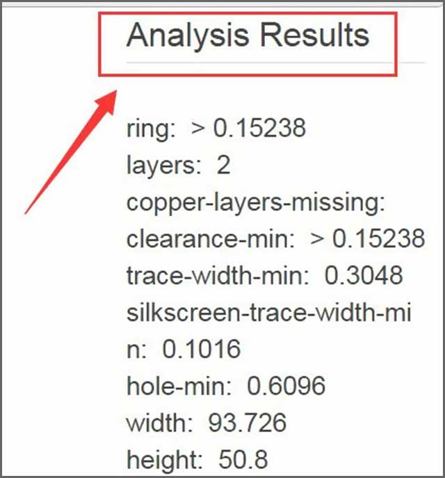
Since the Gerber Viewer is smart, it will perform a DFM check to ensure that the design is adequate. You can use Analysis Results as the parameters of your board during ordering.
It may be best to see an actual video tutorial of how the software works.
Comparison of EasyEDA With Other Software
EasyEDA is not the only PCB design tool out there, but how does it compare with other solutions?
The first important thing to mention is that the tool has a user-friendly interface. That makes it suitable for beginners, but its variety of features is what makes it a great choice for experienced users, too.
EasyEDA also has amazing versatility. You can run it from your web browser if you want to keep things cloud-based. Alternatively, feel free to download a desktop client for Windows, Mac, or Linux. Compatibility with other tools, such as Eagle and KiCad, and the option to import different files only makes EasyEDA more versatile. Unlike other software, you won’t have any platform limitations here.
The tool is completely free to use, and that includes a million of free libraries available. It’s hard to find software that offers so many options in its free version.
The combination of simplicity, versatility, and usability is what makes EasyEDA one of the best choices in the industry of PCB design.
Summary
We hope that this article resolved some important questions you had related to using EasyEDA. If you still have any issues or dilemmas regarding the use of the tool, do not hesitate to contact us. Our team is ready to help you during the entire process. That includes getting your PCB design ready and assembling your board to turn your desires into reality.