
Printed circuit boards (PCBs) are a vital component of most electronic and electrical devices. That’s why designers need to get it right when designing a PCB. To do so, PCB designers add reference points to the PCB design. These reference points help you keep the orientation right.
The purpose of fiducial markers is to provide reference points for imaging systems. Unfortunately, many beginner designers don’t have in-depth knowledge about fiducial titles. For this reason, we’ve prepared this comprehensive guide on fiducial PCB markers. Keep reading to learn more.
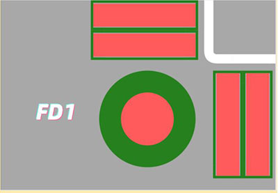
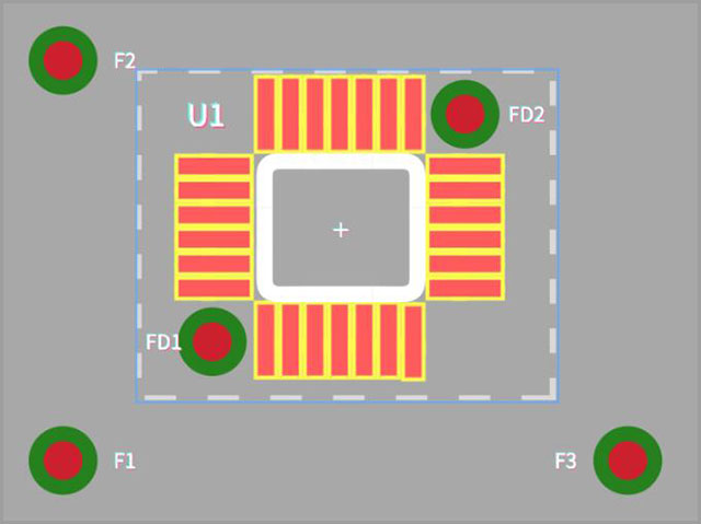
(Fiducial PCB in 2D view)
Contents
- 1 1. What is Fiducial PCB
- 2 2. The Benchmarks of Our Common Fiducial PCB
- 3 3. Why is Fiducial PCB so Important?
- 4 4. When to Use Fiducial PCB
- 5 5. Does Modern Manufacturing Technology Require Reference Marks?
- 6 6. Precautions For Using Fiducial PCB in PCB design
- 7 7. Problems in Designing Fiducial PCB
- 8 Summary:
1. What is Fiducial PCB
The term fiducial refers to a fixed point basis of reference. Its purpose is for comparison. Fiducial markers are surface marks that designers use as directional measures for indexing systems.
In electronic assembly industries that use automation, fiducial markers function as alignment marks that help indexing systems orient the PCB in the right skew and direction. The features allow the vision system to insert components on circuits precisely.
Fiducial PCB markers are a vital aspect of the whole automated process. Therefore, a single mistake in the location of the board or circuit can cause an automation disaster.
The fiducial mark consists of 3 parts.
- Solid copper ring on the top or bottom copper layer
- The circle in the solder mask is the target we need to align
- Option text label on the side
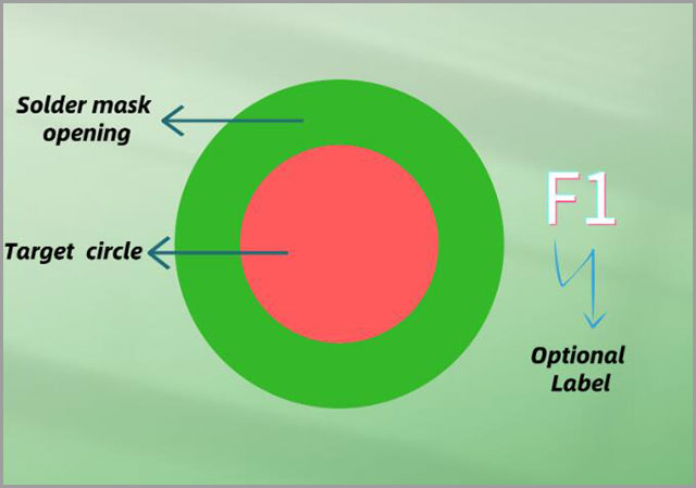
(Picture introduction of fiducial marks)
2. The Benchmarks of Our Common Fiducial PCB
There are three main benchmarks of the common fiducial PCB markers. Let’s look at these benchmarks and where you should place them on the board.
First Datum
The first datum is useful in helping the mounting machines recognize the PCB location in its space. Typically, this benchmark uses the X and Y dimensions.
Second Fiducial Benchmark
This benchmark helps your machine recognize the PCB orientation. It also reveals the PCB’s skew in the clamps. Even a slight rotation of the PCB can result in total ruin of the entire assembly. Fiducial PCB markers ensure that this doesn’t happen. Typically, the machine measures the angle of the board’s rotation to the nearest 0.01 degrees. After that, it compensates all the placements accordingly.
The Third Benchmark
The final fiducial benchmark assists the mounting machine to compensate for shrinks and stretches present in the PCB. In many cases, PCBs over a long distance can vary by slight amounts. For that reason, it’s essential to identify these variations in larger PCBs. Such PCBs experience a more considerable degree of stretch or shrink than their smaller counterparts.
In double-sided SMT assemblies, reflow of the first side in the oven can cause the board to stretch, shrink, bow, or flex. For this reason, you need a third fiducial benchmark to help compensate for that.
3. Why is Fiducial PCB so Important?
Fiducial markers are essential during PCB assembly by picking and placing machinery. In any process that uses automation, precision is vital. In short, machines need to know the board’s exact location and where to put the components. Fiducial markers make sure that the orientation of the board is in the right direction and alignment. By using high-tech cameras, assembly machines can locate the precise location of the board. Therefore, the entire process needs several fiducial marks in an irreversible pattern.
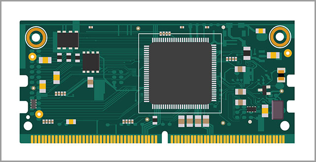
(Using fiducial PCB is essential)
4. When to Use Fiducial PCB
Mass Assembly and Small-Batch Assembly
Fiducial marks are crucial to high volume Bill Of Materials (BOM) of a PCB get fitted onto a board. PCB assembly. That’s because these marks ensure correct parts placement and registration; low-volume assembly doesn’t necessarily require these marks. However, using fiducial characters is always a great idea, whether you are a high volume or low volume PCB assembler. Of course, if you place your parts manually, then PCB marks are entirely unnecessary.

5. Does Modern Manufacturing Technology Require Reference Marks?
The simple answer is yes. Fiducial markers play a vital role in today’s WellPCB. Wne will provide you with one-stop service and high-quality products. You can send us the documents you need to make and get a quote immediately! What are we waiting for? We have ten years of PCB manufacturing technology. Generally, there are two types of fiducial characteristics:
- Global fiducial markers: They are to distinguish the circuit pattern and the panel PCB reference. They should be three grid system-based positioning, wherein the reference point is located at the lower-left end 0,0, And the other two in the X and Y-axis positive direction.
- Local fiducial markers: Positioning requires a higher precision of the position of individual components.
Depending on the size of your PCBs, you can opt to include or omit local fiducial markers. Where the PCBs are small in size, designers can forget local PCBs to increase space for signal traces. In such cases, the assembly machines can use global fiducial points to place SMT components.
Another situation where you can omit local fiducial markers is when using surface mount components with a bigger pitch. Where members rise 1 mm and above, the latest machines don’t need regional fiducial titles to place them on the boards.
(PCB with Global fiducial markers and Local fiducial markers.)
6. Precautions For Using Fiducial PCB in PCB design
Basic principles of fiducial PCB design
For the best results during machine assembly, designers must get fiducial markers right. This section discusses a few essential guidelines to follow when placing fiducial markers in your design.
- Maintain a circular shape when placing the non-drilled copper layer. Keep fiducial markers free from any solder mask.
- The optimal size of fiducial markers is between 1mm and 3 mm. Maintain a clearance area similar to the marker’s diameter.
- When making global fiducial markers, place three markers on the edges of the boards. It ensures the best possible accuracy. Where there’s insufficient space, use at least one global fiducial marker.
- Make sure that the fiducial marker maintains a distance of 0.3 inches from the board’s edge. This distance excludes the fiducial marker’s clearance area.
- For local fiducial markers, place at least two fiducial PCB markers diagonally on the surface-mounted component’s edge plans.
(fiducial PCB design picture)
Optimize the Fiducial Design
There are four factors to consider when designing your fiducial markers. These are:
The Shape: How will your fiducial PCB markers appear? Some machines can recognize a variety of shapes, including squares, diamonds, and hourglasses. Other devices can’t do so. Therefore, it’s best to stick to circular marks, which engines recognize universally.
The Size: Fiducial markers can be a variety of sizes. On average, fiducial pads measure between 1 and 3 mm. The size makes it easy for the camera and equipment to recognize places as fiducial markers.
The size of the fiducial mark on the same printed circuit board should not exceed 25 µm. Wne recommend that the minimum size of the gap area is twice the radius of the center mark.
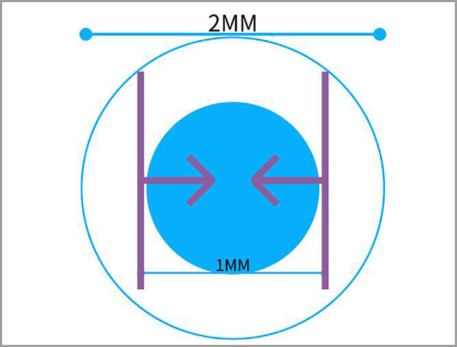
(Recommended standard size-)
Material: Ensure the fiducial pad is the same material as the rest of the board. Make sure that the place is free of solder masks or silkscreen that might cover the markers.
Cutout / Clearance: It’s vital to ensure the appropriate clearance around the pad. That’s because open space around the PCB board makes it easy for the camera to pick up the fiducial markers without interference. Keep the diameter of the clearance at least twice the size of the pad. Don’t worry about the shape of the space. It can be circular or square.
7. Problems in Designing Fiducial PCB
Like all other processes in the assembly of PCBs, it’s possible to encounter problems when designing fiducials. Some of these problems include:
7.1. Position Deviation
Where the fiducials on either side of the board are in a symmetrical pattern, your assembly machine may have trouble raising the incorrectness alarm for the 180-degree placement on an inverted board. Why? When you flip a board 180 degrees in the reverse direction, the symmetrical fiducial marks will interchange their places and deceive your assembly line optical machine.
Even worse, the assembly line continues placing components wrongly without raising the alarm. In the end, you have faulty PCB board manufacturing. As a result, you lose time, money, material, and other resources.
7.2. Direct Light May Cause Bumps
Another major problem with fiducial markers has to do with the harsh direct light from the vision above. This natural light can create bumps that confuse vision detection. That’s mostly due to the uneven solder surface, which creates shadows.
The solution here is to reduce light levels. If doing so doesn’t help, try programming the fiducial with a detection offset in one direction. Consequently, your angle and diffuse the light.
7.3 Do You Need Fiducial Marks on Both Sides of the PCB?
The importance of fiducial markers on a PCB design is unquestionable. Where you have SMD components on each side of the board, you should place fiducial markers on both sides.
Make sure that there’s no solder mask covering the markers. That’s because the vision system should be able to find the fiducials easily. A solder mask on top of the features only makes this harder to accomplish.
Summary:
Fiducial PCB marker placement is a critical part of the WellPCB. Wne will provide you with one-stop service and high-quality products. You can send us the documents you need to make and get a quote immediately! What are we waiting for? We have ten years of PCB manufacturing process. How you do the job can be the difference between a seamless assembly line and a situation where you need to make adjustments continually. Take the time to correctly incorporate fiducials in your designs, even when your supplier says their machines can work without the markers. In case the need arises to rework your plans or test your final product, these markers may prove beneficial.
Would you like to learn more about fiducial markers? WellPCB can offer professional guidance and highly innovative suggestions for your designs. Our leading professionals can also help provide custom PCB solutions for your projects. know more about the defects and probable solutions to PCB problems? Contact us today for a profoundly satisfying co-operation.


