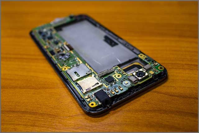
A Printed circuit board (PCB) remains to be a familiar name even though some know them as “printed wiring cards” or “printed wiring boards.” With electronics moving from relays and vacuum tubes to integrated circuits and silicon, electronic circuits’ cost and size started decreasing. The pressure to minimize the size and manufacturing costs of consumer electronic products compelled manufacturers to seek reasonable solutions. This move saw the birth of printed circuit boards.
A PCB is a board that connects several electronic components in one place, allowing power routing across physical devices. PCBs have many different layers in them. To the uninitiated, these types of coatings can be a little bit confusing. However, once someone gets a basic understanding, then everything appears simple. This article looks at matters concerning PCB layers, such as the types, stacking methods, layer connectivity, and proper application of these layers.
Contents
- 1 Common Types of PCB Layers
- 2 Common PCB Layer Stacking Methods
- 3 PCB Layer Connectivity
- 4 How to Determine Your PCB Layer
- 5 PCB Layers–How Should We Apply These Layers Properly in the PCB Layout?
- 6 PCB Layers–Purpose of Multilayer PCB Board
- 7 PCB Layers–How Do We Align When Making Multilayer PCBs?
- 8 Customizing the PCB Layers
- 9 Summary
Common Types of PCB Layers
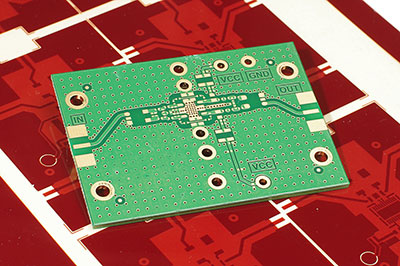
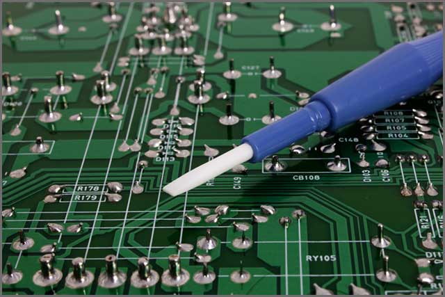
Printed circuit board layers consist of 7 categories. They include signal layers, mechanical layer, inner planes (ground layer/inner power), silkscreen layers, solder mask layer, system work layer, and others.
Signal Layers
They include the bottom layer, top layer, middle layer 30, intermediate layer 1, and 2. They find their use in the placement of components and routing. Here, the wires and other objects on the surface consist of copper cover.
Mechanical layer
These types of coatings consist of indicative information regarding the board and means of assembly. Such include physical dimension lines, data, dimensional markings, through-hole information, and assembly instruction, among others.
Internal planes
Also referred to as the inner layer, these find their use in the arrangement of ground wires and power lines. The objects or lines at these levels are copper-free or harmful in other words. They play an active role in distributing power and ground in a PCB.
Silkscreen layer
These layers find their use in drawing the outline of components, text information, or the number of elements on a PCB.
Solder mask layer
Green in color, they protect the traces from shortening, mainly when PCB accumulates debris.
System work layer
They find use in displaying electrical connections between pads, components, and vias.
Others
Other types of coatings include keep out layers/sheets, split planes, solder paste, and multi-layers, among others.
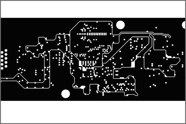
Common PCB Layer Stacking Methods
Stacking is necessary during the manufacture of PCBs. But what is stack-up anyway? Stacking is the arrangement of insulating layers and copper layers that make a printed circuit board before the design of the board layout. Apart from allowing one to get more circuitry, there are other advantages associated with stack-up.
For instance, PCB stack-up helps in balancing the need for efficient and low-cost manufacturing methods. Additionally, it contributes towards the minimization of a circuit’s vulnerability radiation and external noise. Furthermore, a good PCB layer stack-up enhances the Electromagnetic Compatibility of the design also.
There are several PCB layer-stacking methods. But some of the most common PCB layer stacking methods include 4, 6, and 8 PCB layer stacking. It’s simple. Layer stacking is where a PCB maker decides whether to manufacture PCBs containing four layers, six layers, or eight layers; simple as that.
PCB Layer Connectivity
For useful functionality, there is a need to connect different layers of the printed circuit boards to become a single unit. Without connectivity, a conductive connection between the layers of the printed circuit board won’t be achievable. When it comes to a printed circuit board, there are three main types of PCB layer connectivity. They include Through-hole, Blind via, and Buried via connectivity.
In the design of PCBs, there’s a via consisting of two pads that are in corresponding position different layers of board electronically connected by a hole through the board (therefore, the term through-hole). Blind vias only connect layers on one side of the board while buried vias only connect internal layers. Blind vias do not get exposed to the surfaces of the board.
How to Determine Your PCB Layer
PCB layers determine the capacity and power of a printed circuit board. A lot of people seem confused as to whether a one-layer printed circuit board will suffice, or they are better off dealing with four or even six-layered PCB. While the number of layers at most times depends on your budget, there are other determining factors too.
Other determining factors that you need to consider when choosing the number of layers that your PCB should have include:
- The applicability or usage of your PCB
- The type of operation or frequency needed
- Your total budget for the intended project
- How fast you need the PCB
- Density and signal layers required in your PCB

PCB Layers–How Should We Apply These Layers Properly in the PCB Layout?
Immediately after the design of PCB is complete, the next step is the placement of different layers on the layout. Incorrect installation of these layers may result in a board whose functionality isn’t up to the required standards. There is, however, an effective way of placing these layers correctly on the PCB layout.
The application of layers in the manufacturing of PCBs, there are high chances of layout failures, which can go a long way into negatively affecting the final product’s functionality. There are several PCB layout is carried out in two steps: the laminating step and the lay-up step. The two processes are almost the same. Here, a mechanical press presses all the layers together on the layout. At this point, pins get punched to the sheets for them to remain correctly aligned. Depending on the technology at hand, these pins are then removed, leaving the layers sitting on the layout.
PCB Layers–Purpose of Multilayer PCB Board
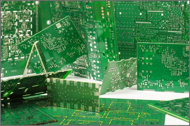
A multilayer PCB is a board whose make consists of three or more conductive layers of copper foil. They appear as some layers of double-sided PCBs that are with some layers glued and laminated together using layers of heat-protective insulation in between them. There are several benefits associated with multilayer printed circuit boards, as highlighted below.
First, multilayer PCBs are small in size than other PCBs with the same functionality. Small size is beneficial since modern electronics in the world seem to be gravitating towards smaller, compact, and powerful gadgets. Secondly, they are lightweight, meaning they are highly mobile. Thirdly, they are highly durable and high in quality due to the amount of planning that goes into their creation. Lastly, they are more flexible and powerful.
The above advantages make multilayer PCBs increasingly useful in a host of applications. For the above and plenty of other minor benefits, it is no wonder to see an increasing number of sectors choosing to use them.
PCB Layers–How Do We Align When Making Multilayer PCBs?
The process of alignment when making multilayer PCBs isn’t as difficult as such. First, each of the layers undergoes a cleaning process to make them ready for adjustment. The holes that had been drilled earlier find use in aligning the inner and outer layers of the PCB. For layer alignment to be a success, a technician will place them on a particular type of machine commonly referred to as a visual punch.
This machine drives a small pin down through the holes to line up the layers of the board. After that, there is another machine designed for optical inspection to ensure that there are no defects at all.
Customizing the PCB Layers
To a certain extent, people are the critical factor in determining whether you can get good service. Besides our excellent manufacturing capabilities, we at WellPCB have in place a passionate and dedicated team ready to assist you in reaching there. Unrivaled customer service is what we always pursue. Taking the manufacture of PCBs as a lifetime career, we work effectively and take pride in producing PCBs in the way you want them.
We hold customers’ confidentiality to high standards and have in place a Non-Disclosure Interest with each customer. Using well-equipped machines coupled with international standards, we offer customized services to meet the custom requirements of our customers. We run an onlie quoting and tracking system to make it easy for you o track and follow your order. Still, our prices are the most competitive in the industry. Are you in the market for a reliable, dependable, and trustworthy PCB maker? Look no further than WellPCB.

Summary
Printed circuit boards are devices that connect several electronic components, allowing routing of power between physical devices. A majority of electronic gadgets people and industry use daily consist of PCBs in them. These PCBs consist of some layers. There are those with two coats, four layers, six layers, and so on depending on use and budget, among others.
For useful functionality, these stacked layers require excellent connectivity and alignment. There are a majority of companies currently dealing in the manufacture and assembly of PCBs. But if you are in the market for a firm that you can trust for all your PCB needs, look nowhere else; need to know about ordering custom PCB Circuit boards online. FOR the PCB board you need, you can contact us at WellPCB is here to assist you.


