Contents
What Is a PCB Prototype Board?
Before we get into the details of using a PCB prototype board, it is essential to understand what a PCB prototype board.
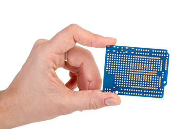
A PCB prototype board refers to a simple printed circuit board with several receptacles with a grid where you can place components and wire them together in an organized fashion. These prototype boards enable the designer to reduce solder connections and the number of wires you need to connect different circuit components. The panels can provide power and bussing, making it easier for multiple parts to connect to the power bus if necessary.
Designers use PCB prototype boards to prove the concept of an electrical circuit before sending the final product for manufacturing. Electrical circuits tend to be highly sensitive to various component values leading to system performance variations. For this reason, it is essential when designing products to explore different scenarios of circuit performance.
By using a PCB prototype board, you can make different iterations and changes without wasting development time and increasing the cost of redesigning the entire PCB.

Varieties of PCB Prototype Boards
PCB protoboards come in different varieties that you need to know when learning how to use the bare PCB, it may also include PCBA depending on what you want the PCB factory to do for you. This is why you should choose a PCB factory that will produce your PCB prototype board. In this section, we will discuss two of the most common PCB prototype boards in the market. While both varieties feature a sheen of resin with grid holes, the underside’s conductive power is different.
1. Perf Board
Perf boards, as we mentioned earlier, are among the commonly available type of boards in the industry. Another common name for these prototype boards is the pad per hole design. Each hole has a copper conductor pad. With this connection, it is possible to test connections by simply running solder between individual pads. Moreover, you can run multiple wires between the pads on the perf board.

2. Strip Board
Like perf boards, stripboard prototype PCBs feature an individual hole set up. Rather than each perforation featuring a single conductor pad, there are strips of copper running parallel under the board’s entire length. These strips connect the holes.
The strips in this prototype boards act as substitutes for wires, and you can break connections if you wish.
Both perf boards and stripboards can work wonderfully as planning boards. Stripboards are also excellent for planning simple circuits as a result of the existing copper connections. Whether you choose to work with perf boards or stripboards, however, you’ll still need to use protoboard soldering and wires when testing the potential board.

The Planning Stage
Even if you’re a seasoned engineer, you don’t want to jump straight into building a PCB prototype board without proper planning. Even learners on how to Use the PCB prototype board understand the importance of starting with a plan.
A PCB prototype board may be a lot less costly than the actual PCB, but its configurations are more permanent. Don’t start putting components into place before spending time on the planning stage if you’re looking for the best results.
So how do you go about the planning phase of a PCB prototype board? Well, you can use either of two ways. First, you can use board-planning software on your computer to visualize circuits before you put any components down.
Bear in mind, however, that some applications are suitable for only one type of protoboard, while some will work for both perf boards and stripboards. That’s why you need to plan your protoboard purchases appropriately.
You can also opt for a less digital option when planning your prototype board layout, such as a graph paper. In this case, everywhere lines cross, that is where the hole will be on your board. Once you are identified the holes’ location, you can then draw the rest of the connections and components. Do not forget to indicate where you plan to break the strip case you intend to use a stripboard.
Each of the above methods has its pros. For instance, a digital program allows you to edit your ideas faster. However, when you draw things by hand, you orient yourself with the project better. Regardless of the method you choose to use, never skip the planning stage. You will save yourself plenty of time and energy when you move into the actual process of building your protoboard.


Cutting the Protoboard
In most cases, when you are using the prototype board, you will not need a whole sheet. PCB boards usually vary, so chances are you will need to cut a piece.
This process can be complicated, so you need to be very careful. Part of the reason for the difficulty in cutting is the material that makes the protoboard. Resin can make the protoboard easy to crack, so designers need to exercise caution.
So how do you ensure that prototype boards do not crack when you are cutting them? The key lies in using the right tools, i.e., a straightedge and a sharp knife. Use the edge as your guide to scoring the line along which you wish to cut the board. Repeat the same action on the other side before setting the prototype board on the edge of a flat surface, such as a table. Now you can snap the board cleanly along the marks you made.
Other tools that you can use include band saws, but these usually increase the probability of damage.
For cleaner breaks, make scoring marks along the holes in your board since the holes make the protoboard less stable, reducing the risk of snapping.

Converting Breadboard to Stripboard
Most people who are dealt with PCB prototyping are familiar with PCB breadboards. Breadboard prototype PCBs are ideal for developing designs because they allow you to move and change components out while setting up your plan. Moreover, you can reuse breadboards.
You can easily move them to the stripboard when you need to test components in breadboards further. Naturally, stripboards and perforated protoboards have fewer limits since you can create more connections.
When planning to convert from breadboard to stripboard, ensure that you purchase a stripboard that comes with a matching orientation. Also, you can break the stripboard traces, which we will discuss in the following section.

Breaking Stripboard Traces
Earlier in this guide, we mentioned that stripboard PCBs have copper strips along the bottom. These copper strips serve as connections. But since you do not want all your components connected all the time, you will sometimes need to break these strips.
Fortunately, it is easy to handle this process with only a drill bit. The only thing you need to do is press a tip of a 4mm bit against the hole where you intend for the connection to break. As you twist the bit and apply a little pressure, you will be able to cut away the copper, ending up with isolated strips.
Of course, there are other specific tools you can use for the process, but the DIY approach is just as effective.

Summary
Knowing how to use a PCB prototype board is vital for any engineers who intend to design and test PCBs without incurring the cost of printing. As long as you have a prototype circuit board, you can make immense progress to the complete product.
Of course, it helps partner with a reputable PCB manufacturing company to create great designs and end up with the perfect product. That is where WellPCB comes in. At WellPCB, we have a large team of highly experienced professionals ready to serve you. Over the years, we have provided exceptional Contact us today for a quote.
