Contents
Insufficient Hole Filling
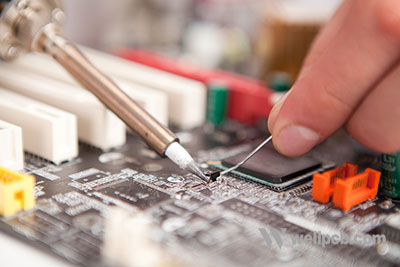
When it comes to PCB board soldering, insufficient holes are among the most common problems on PCBs consisting of pre-drilled holes used in mounting parts to the board. In short, when there is a lack of sufficient solder required to fill the holes drilled on the board, then under-filling takes place in the trenches, meaning that once the solder cools, it will not stick to the printed circuit board properly.
Luckily, though, cases of insufficient hole filling can be fixed. As a PCB designer, the best way of fixing such an issue is to ensure that you run your board through several pre-solder checks. Check for the type of flux you are using, not forgetting to ensure a sufficient volume of flux to cover the whole board. Additionally, it is essential to ensure that the pins’ diameter and the size of the pads match.
A Gap in the Solder Joint
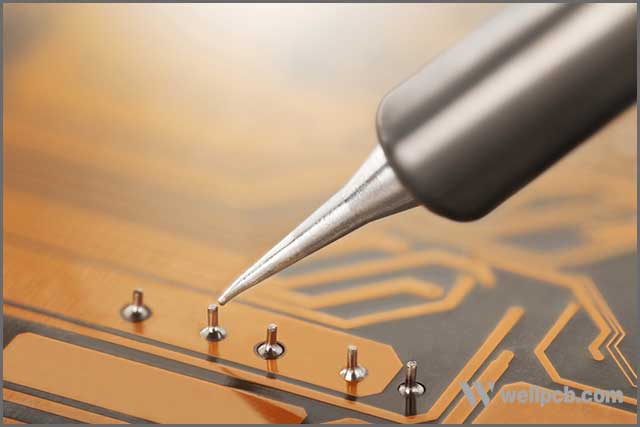
When it comes to soldering PCBs, ensuring that that the solder joints on the board are in the right way is of importance in electronics construction. Weak solder joints with gaps in them will either make the equipment not function as desired or a possibility of the solder joint falling intermittently. Unfortunately, differences in the solder joint are typical wave soldering defects that plenty of printed circuit boards soldering technicians face.
1. All is not lost, though, as there are a few pointers that can help designers develop solder joints. Here are some of them:
2. Ensure that the entire surfaces that need soldering are free from greaser and clean
3. Ensure that the components to be soldered are tightly secured to avoid movement during the soldering process as this may bring about gaps in the solder joint
4. Before allowing changes, make sure that the solder on the joint cools
5. As soon as you get rid of the soldering iron immediately to avoid cases of dry bones, hence gaps in the solder joints
Pad Pitch
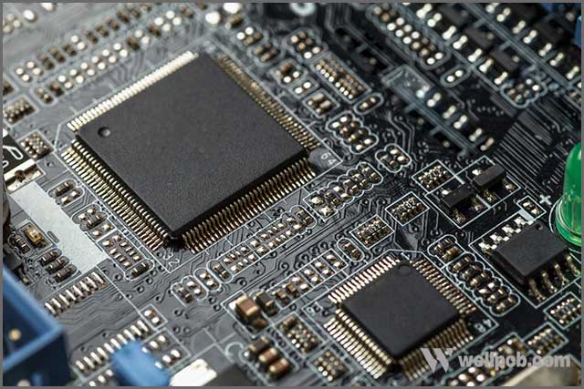
In general, if there’s a way to avoid drilling holes on your printed circuit board, then you should. But at times, you cannot prevent drilling holes on your board. Most of the time, you will make holes on the PCB, which is when you require a pitch pad. Pitch pads have got materials that melt upon composition. Again, when it comes to PCB board soldering, the best pitch pad materials to use becomes a big challenge. Some of them are not good and up for the task.
However, to avoid the above issues, it is essential to take some considerable time to lay down pitch pads correctly before beginning the soldering process. Additionally, as a designer who wants to get excellent results, you may have to go for pitches that are as low as 0.55mm.

Application of Solder Resist
Solder resist is an integral part of PCB technology. Solder mask or solder resist on the printed circuit board does perform several essential functions worth noting. For instance, solder resist protects a PCB from mechanical challenges and corrosion. It also prevents the board from mechanical problems during the process of wave soldering.
However, when it comes to wave soldering of PCBs, the application of solder resist is a big challenge that faces plenty of PCB board soldering technicians. Only the areas that require the welding should be left exposed for wave soldering to avoid defects on the board. But again, reduced application of welding resist is a common defect that plenty of PCB designers face.
Discoloration of Solder Mask
Even though the stain of the solder mask may come as a cosmetic issue, its causes need to be investigated thoroughly by your manufacturer. Finding discolored costumes can be easily identified on your PCB, on the solder resist, the conveyor belt, or even in the wave soldering equipment. Common causes of discolored solder mask include using different flux components, mixing several batches of PCBs during wave soldering, and changing the type of solder mask or its thickness halfway through the process.
Discoloration of the solder mask is also a familiar wave soldering defect that plenty of printed circuit board manufacturers encounter. To ensure that instances of solder mask discoloration do not occur, manufacturers need to watch the range of PCB solder temperatures they use, avoid the use of different flux materials, and stick to the same solder mask thickness.

Poor Penetration
Flux must be there in the plated through-holes to effectively enable a solder joint to form at the top of the board. If you achieve perfect pre-heat conditions, then the flux penetration will be useful, resulting in a high-quality printed circuit board. Poor penetration may be caused either by inadequate pre-heating or reduced application of flux.
To do away with poor penetration cases –especially if it is flux-related- it is essential to ensure that you use the right amount of flux instead of using low flux. Additionally, enough pre-heating is necessary to ensure that the material penetrates the board’s intended areas.

Lifted Components
Also referred to as tombstones, raised components are the aerial parts of a printed circuit board during wave soldering. Some of the most common causes of raised elements or tombstones include:
1. Use of ingredients with some varying needs for temperature and solder type.
2. Wrong lead lengths and trying to undertake wave soldering, especially on flexible PCBs that will bend like the rest of the parts stay flat.
To properly correct the printed circuit board’s flexing, you need to double-check the type of PCB that you are using in addition to its thermal forces. If you want to address incorrect lead lengths, you may have to hit the solder bath to push them out through the through-hole. Lastly, it’s essential to check your PCBs thermal tolerances and all its parts. Components with different solderability temperatures may lift during wave soldering. But to avoid such cases, it’s vital to ensure that the ingredients used have equal requirements.
Solder Ball Phenomenon
Solder balling comes in as another challenge that PCB designers face, especially the process of wave soldering. The solder balling occurs when small particles of solder get to re-attach themselves. Especially close to the leads of the printed circuit board. Some of the underlying causes of welding balling include using a high-temperature solder. Falling solder when separated from the board, and liquid gases that spit back to the board.
There are means to fix ordinary solder balling issues. However, one of the best ways to fix ordinary solder balling challenges is way back when designing the PCB. When selecting the solder mask that you want to use when creating your PCB. As much as possible, try and look for one that comes with little chances of allowing the solder to stick to it. Additionally, you may also need to check the amount of air that flows in the solder tank and the ratio of nitrogen present in the environment of your solder tank.
Generating A Solder Mark
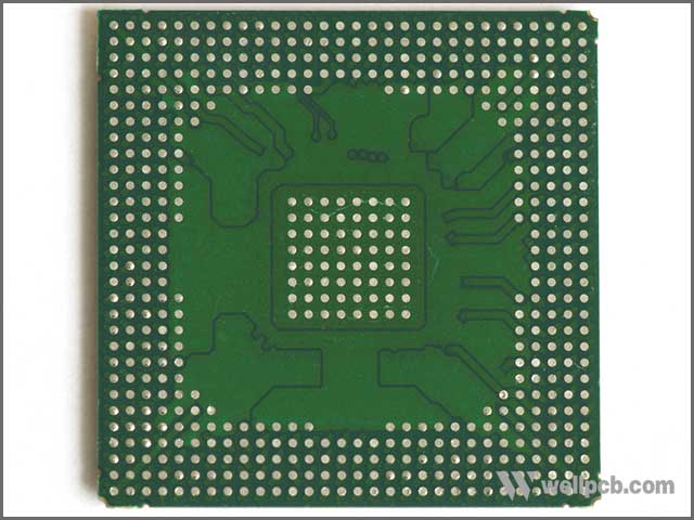
When it comes to the manufacture of printed circuit boards, solder marks are collective in position referencing. Solder masks consist of small filled circles of copper and a clear area from the solder resist layer. At times, it becomes hard generating a solder mark when undertaking wave soldering.
To ensure that position referencing is done correctly, it is essential to use the right machines or equipment to generate solder masks for position reference.
Summary
So there you have it, ten current wave soldering defects and their solutions. The above are common issues that have a high chance of ruining an otherwise excellent PCB design. But again, you need to be aware that the above cases may not always emanate from you.
At times, your manufacturer may be at fault if you are looking for a designer in the market to assist you in your next printed circuit board project. Then WellPCB is your ideal choice. We at WellPCB can resolve any wave soldering defects and other problems that might come up during manufacturing. Feel free to contact us at your earliest convenience. We will be happy to discuss all the questions you may have.
