Contents
1. PCB vs PCBA– What is a PCB?/PCB meaning
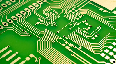
A PCB (Printed Circuit Board)is a compulsory module that we use to connect electrical components.
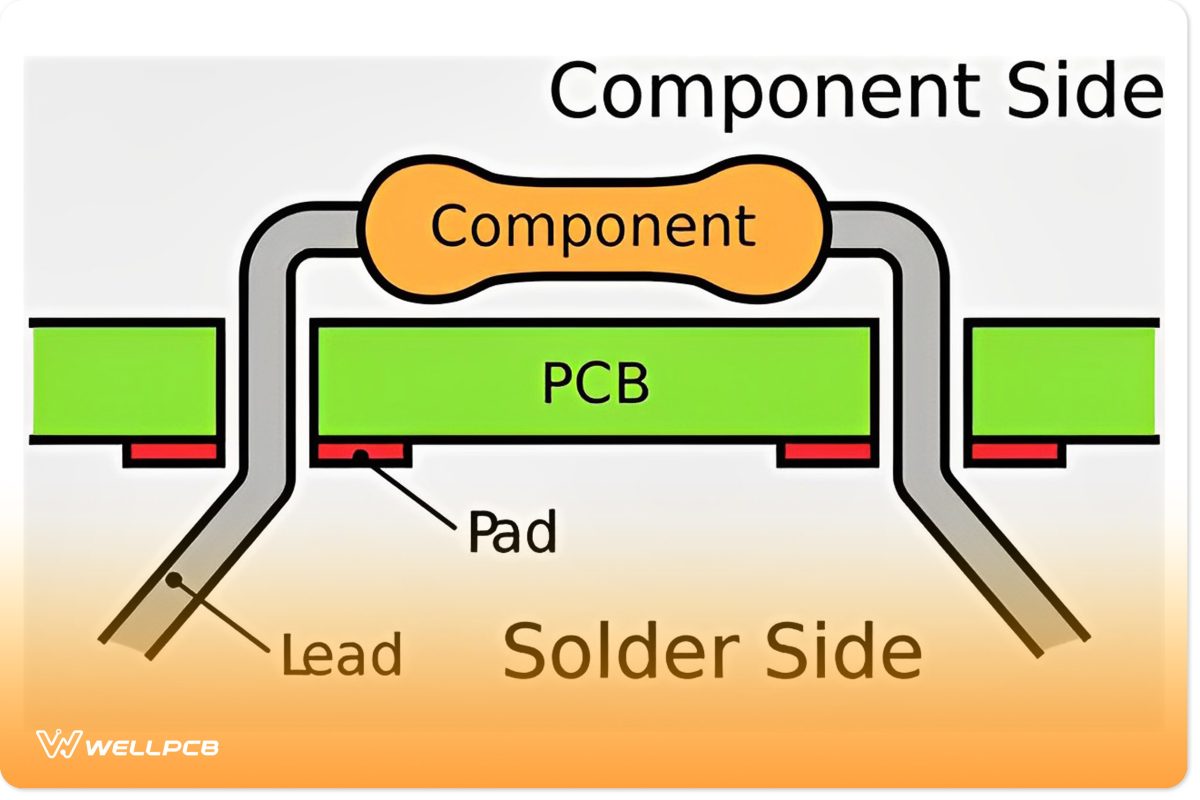
The board uses pads, conductive traces, and other copper-etched features to facilitate electrical device functions effectively.
Experts then place one component individually on the substrate and solder to the appropriate interconnecting circuits.
The substrate has ‘contact fingers’ along the edges that connect to external devices or other PCBs.
The majority of electrical devices we use today run off PCBs, from virtual devices like radios and pagers to sophisticated instruments like radar equipment and computers.
The PCB circuits can perform single or multiple functions as desired.
1.1 PCB vs. PCBA—Types of PCB
Now that you know what a PCB is, you should know we have more than one PCB. There are mainly three types of PCB, and they are:
Single-sided PCB
A single-sided PCB has all its components installed on only one side of the board. Proper construction ensures that all components are well-sited and secured.
Double-sided PCB
A double-sided PCB is used when the components to be placed are too much for a single side.
Drilling holes straight through the substrate in strategic positions enables electrical connections between both sides. Internal pores coated with a conductive material to achieve efficient current.
Multi-layered PCB
Consecutively printing layers of circuitry design a multi-layered board on each other, separated by layers of insulating material.
The fabricator connects the components on the surface to the appropriate circuits by drilling plated holes into the desired layer.
PCBs are crucial to every aspect of our daily life. Our appliances and resources to keep our lives running rely on printed circuit boards. Read on to learn how this fantastic technology design is the design.
1.2 Design
The design of a PCB offers limitless possibilities. Each board’s design allows it to perform a specific function for a unique product.
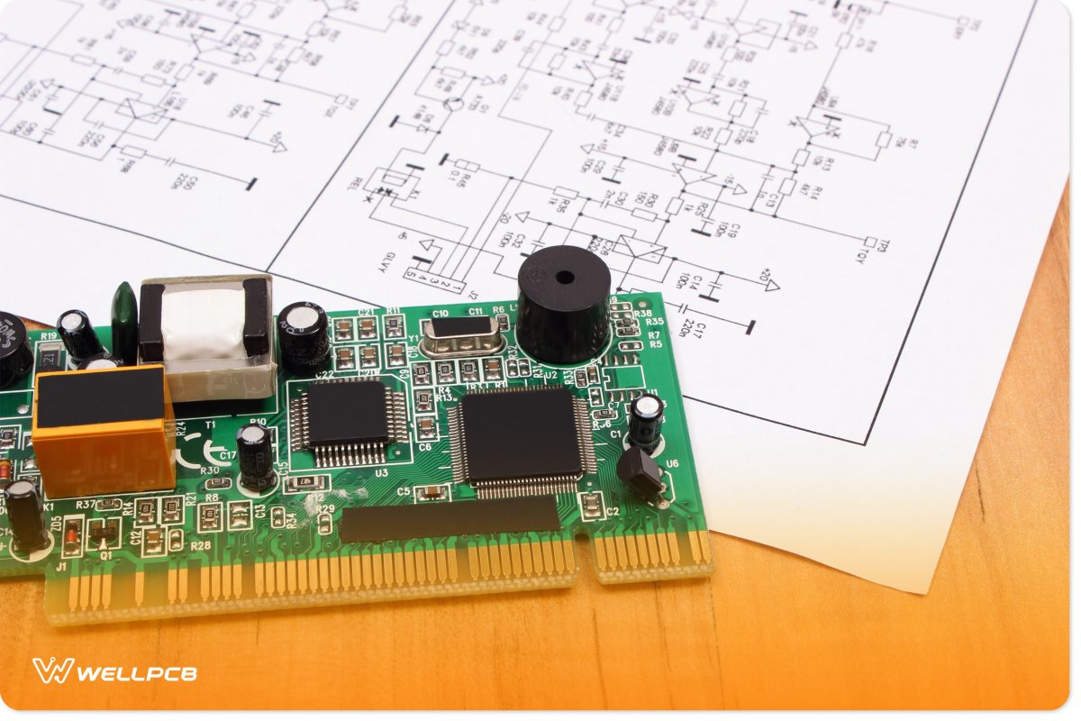
Experts employ CAD (computer-aided design) systems and dedicated software to lay out the board’s circuit pattern for PCB design.
A board designer must maximize the allotted space for the board and achieve the desired functions.
After the fabricator has laid out the circuitry, a printer etches a negative image (mask) on a transparent plastic sheet with precise dimensions.
The cover colors are not part of the black design, and the circuitry appears clear against the background. The locations for contact-point holes are also easily distinguishable from the overall design.
1.3 PCB vs. PCBA–Common Materials Used
You already know the critical processes involved in PCB design. It is amazing how a small tech can have such a powerful impact.
The importance of PCBs means that only the best and most durable material is used in their creation. Read on to find out what makes up the PCB.
The substrate is usually a glass fiber-reinforced epoxy resin in PCB manufacturing and printing.
High-end board production involves pairing the glass fiber-reinforced epoxy with a copper foil bonded to one or both sides of the substrate.
Boards produced using paper-reinforced phenolic resin with a copper foil bonded to it tend to be less expensive.
You can find these PCBs in most household electrical devices and appliances.
The board’s printed circuits consist of copper. The fabricator etches or plates it onto the substrate’s surface in the desired pattern.
To prevent oxidation of the copper circuits, manufacturers coat them with a layer of tin-lead, which provides the required protection.
The contact fingers on the outer edges of the substrate are first plated with a tin-lead mixture, then nickel, then gold for maximum conductivity.
We have covered just about everything there is to know about PCBs. However, that’s just one side of the coin.
The next chapter will delve into what Printed Circuit Board Assembly(PCBA) is and why it’s so important.
2. PCB vs PCBA– What is a PCBA?
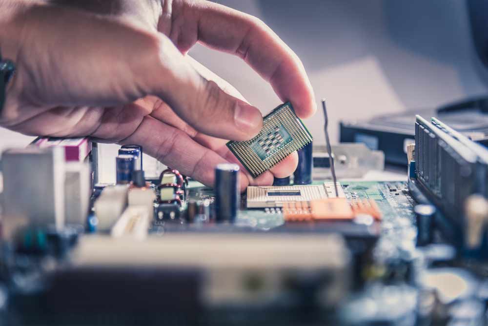
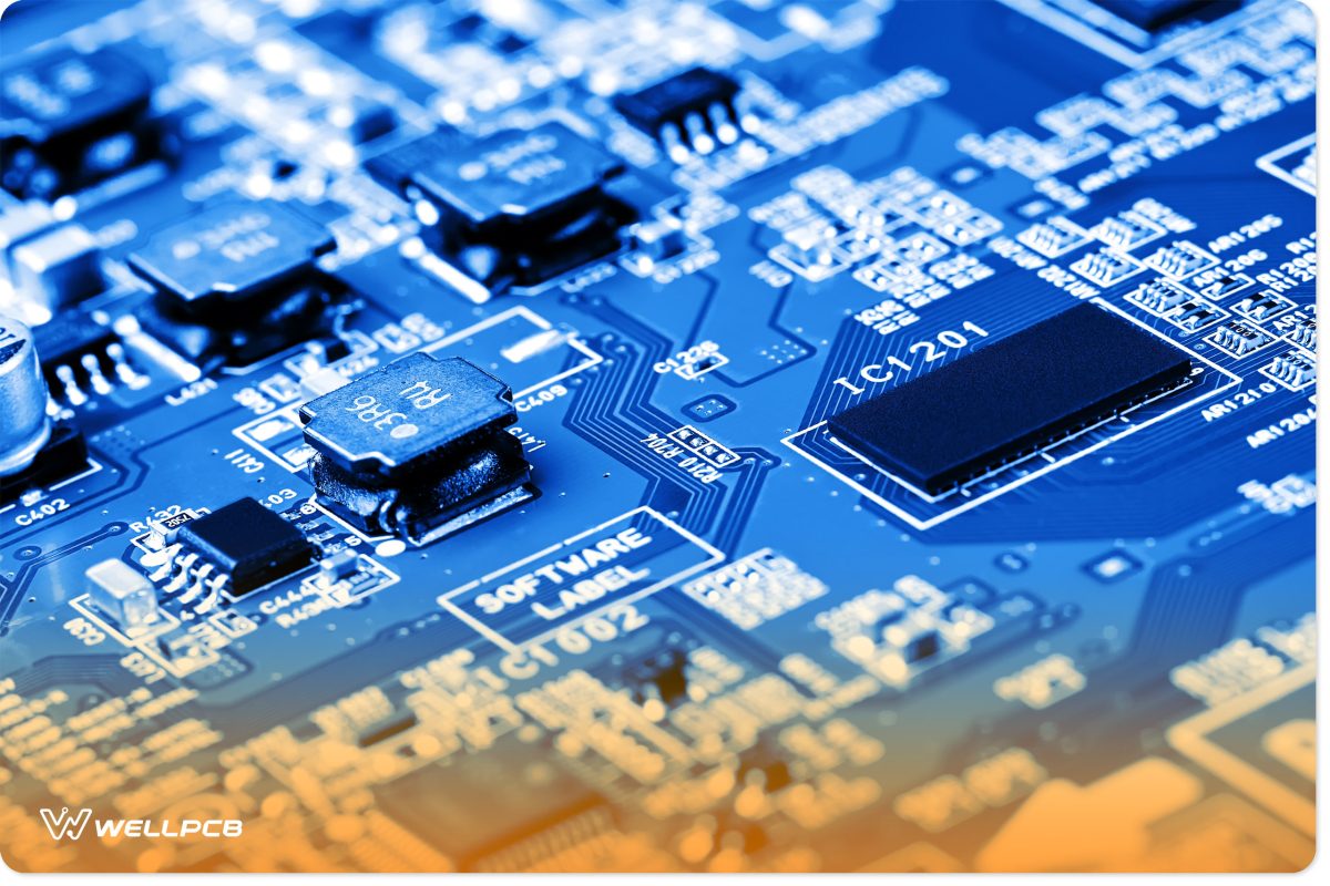
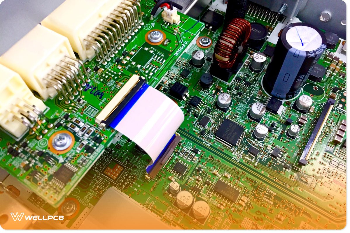
A PCBA stands for Printed Circuit Board Assembly. It refers to the board obtained after completing all printing and mounting operations.
When choosing PCB vs. PCBA, the critical point is that a PCB is just a board with circuitry printed. PCB Rapid Prototyping.
3D PCB Printing makes the PCB and does the Printed Circuit Board Assembly PCBA is the complete package; it has been fitted with all necessary components and is ready for deployment for its desired purpose.
A PCB Rapid Prototyping. 3D PCB Printing makes the PCB, but it also does the Printed Circuit Board Assembly (PCBA will undergo a process known as reflow furnace heating to help establish a mechanical connection between the board and its accompanying components.
The manufacturer can then mount the components onto the PCB Assembly. These components include capacitors, inductors, resistors, diodes, triodes, and modules.
3D PCB Printing makes the PCB and does the Printed Circuit Board Assembly (PCBA manufacturing.
PCB Assembly Is a delicate process, and everyone should take it seriously.
Only skilled technicians and specialized computer systems can carry it out.
The next chapter talks about the assembly methods used in PCB Rapid Prototyping.
2.1 PCBA
There are two primary methods for assembling components in a PCB Rapid Prototyping.
3D PCB Printing makes the PCB and does the Printed Circuit Board Assembly (PCBA). These are:
·Surface-Mount Technology (SMT)
This method of PCB Rapid Prototyping, 3D PCB Printing, not only makes the PCB but also does the Printed Circuit Board Assembly (PCBA), which is highly suited for small circuits and components.
It is a fully automated SMT. This will make it easy for a pick-and-place machine to place the details on the PCB (PCB Assembly process that features three main steps).
First, the printed circuit board receives a generous application of quality solder paste from the printer. Next, all the necessary components are installed in their respective locations.
Finally, the board passes through a 500-degree furnace that liquefies the solder past, sealing all parts.
·PCB vs PCBA–Thru-Hole Device (THD)
THD technology results from a combination of manual and automated operations. It also involves three execution steps.
A technician manually places the electronic components on the board during the first step.
The second step involves inspecting and rectifying all set components. In the third step, the whole PCB Assembly undergoes wave soldering.
Wave soldering passes an assembled board through a wave of liquid solder at 500 degrees Fahrenheit.
3. PCB vs PCBA
So far, we have learned what a PCB is and how PCB Rapid Prototyping works. 3D PCB Printing makes the PCB and the Printed Circuit Board Assembly (PCBA) work.
With this critical knowledge, it’s time to discover the differences and what sets them apart.
3D PCB Printing makes the PCB and does the Printed Circuit Board Assembly (PCBA); one needs to note the most distinguishing factor.
A PCB is only a blank circuitry board, while a PCBA is a fully functional board with the required components attached.
We can view the Printed Circuit Board Assembly (PCBA) as such after the manufacturer has fully developed the PCB.
3.1 PCB vs. PCBA—Differences
It is essential to spot the differences between PCB vs. PCB Rapid Prototyping.
3D PCB Printing makes the PCB and does the Printed Circuit Board Assembly (PCBA). The significant differences are:
·Manufacturing Procedure
While a PCB Rapid Prototyping. A PCB (printed circuit board) is easier to produce since it requires no assembly.
3D PCB Printing creates the PCB, but it also complicates the Printed Circuit Board Assembly (PCBA) due to the various components that need to be attached and the subsequent furnace soldering of their connections.
· Cost
For the same board, the Cost of manufacturing a PCB is far lower than the Cost of producing a unit of PCB Rapid Prototyping.
3D PCB Printing not only makes the PCB, but it also does the Printed Circuit Board Assembly (PCBA.
The additional components associated with the PCBA carry substantial costs that cost the overall Cost of the completed PCBA.
·Functionality
A PCB is a ‘blank board.’ It has no components that facilitate the passage of electricity through it.
PCBA, on the other hand, has all the essential details attached and is ready for deployment
·Packaging
Manufacturers pack PCBs using vacuum packaging and PCBAs using compartmental or antistatic packaging.
3.2 PCB vs. PCBA–Applications
Our cars, media devices, and home appliances would all be imaginable. Packaging is without printed circuit boards (PCB)and printed circuit board assemblies (PCBA).
The applications of PCB packaging are across all electrical devices that we use, from simple pagers and alarms to complex machinery like MRIs and radar equipment.
Modern society as we know it runs on the back of production film work that you require to manufacture PCBs.
As complexity increases, the boards are optimized to be smaller and more powerful.
We are even developing 3D circuits that offer extraordinary capabilities for such a futuristic design.
How Do PCBs and PCBAs Relate to Each Other?
People sometimes use the terms PCB and PCBA interchangeably (erroneously). While these concepts are related, they’re not essentially the same.
The PCBA cannot exist without the PCB, which is its core part.
Ultimately, the PCB is a clean slate or precursor to what will eventually become a PCBA.
Only after a manufacturer situates, fits, and applies the necessary components can you consider a PCB a PCBA.
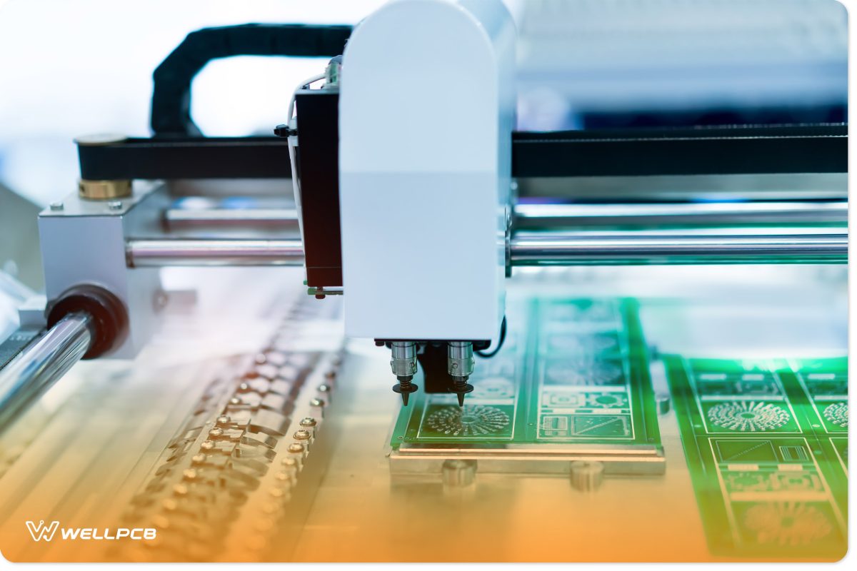
Soldering Iron Tips Automated Manufacturing
What is the Difference Between PCBA and PCB
Ultimately, the PCB is the base product, while the PCBA is its completed form.
Implementations such as motherboards, power supply boards, and even single-board computers (SBCs) can be considered PCBAs.
All these examples would not exist without the PCB.

PWB vs. PCB vs PCBA
As with PCB and PCBA, people often use the term printed wiring board (PWB) inappropriately. PCBs and PWBs are fundamentally the same in purpose and usage.
However, their structures are slightly different. PWBs are a legacy technology. Like PCBs, they have no electronic components but have copper traces or wiring in place.
In the past, manufacturers and fabricators did not have the technology they have today. They could not automatically draw and etch circuits into boards.
As such, they had to manually wire the board and then attach electronic components to it point-to-point.
Hence, they referred to them as PWBs and not PCBs.
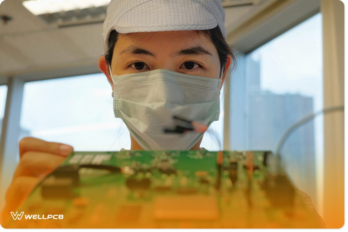
Female Electronic Manufacturing Employee Clean Suit
PWBs typically consisted of an epoxy glass substrate. After the component attachment process, we could refer to them as printed wiring board assemblies (PWBAs) or just printed wiring assemblies (PWAs).
These are essentially the same as PCBAs.
PWBs were eventually phased out and replaced with modern-day PCBs.
In contrast to PWBs, engineers perform much of the PCB design and fabrication process through computers.
Most of the fabrication process is automated, allowing manufacturers to mass-produce PCBs.
The fabrication process isn’t the only big difference.
PCBs can accommodate more components than PWBs. Thus, PCBAs are far more advanced than PWBAs.
Despite some key differences, some may still refer to PCBs as PWBs. However, as you can see, it’s a deprecated term.
Choosing Between PCB and PCBA
Now that you’ve explored the differences and similarities between the two technologies, it’s important to examine what circumstances each can be used for.
Printed circuit boards do not have electronic components, making them ideal for educational purposes. Breadboards and prototype boards may be best for beginners.
However, intermediate and advanced electronic/electric engineers may move on to practicing soldering and electronic component placement on proper PCBs.
Similarly, hobbyists can use plain PCBs for their home projects.
On the other hand, PCBAs are typically intended for specific use cases.
While you can still use them for educational purposes, they’re far more appropriate for electronics. PCBAs are typically embedded in larger devices such as computers.
As mentioned, you can also use them as single-board devices such as SBCs and microcontrollers.
Choosing a PCB or PCBA Manufacturer
You need to pick your PCB manufacturer carefully. Factors that must be considered include:
Source of Materials:
While the source ultimately affects the quality, it isn’t the only reason to worry.
Does your PCB manufacturer source materials ethically?
What’s the environmental impact of the materials or the sourcing process?
These are just a few of the questions you should ask when vetting PCB and PCBA manufacturers.
Standards, Credentials and Certifications:
Establishing that the manufacturer is accredited and registered by the relevant governing bodies would be best.
Some compliance and certifications you should look for include:
- ISO 9001
- RoHS
- IATF 16949
- IPC-A-610F
In addition to this, you can also try to consult with the candidate manufacturer’s past clients. Some reviews and testimonies are available online.
Technology, Infrastructure, and Expertise:
Does the manufacturer have the technology to accommodate your orders efficiently?
Some manufacturers offer tours allowing you to see the equipment in real life, while others have videos and virtual tours.
You can also visit their website to see the specifications of their machinery and equipment. It’s best to ascertain whether your candidate manufacturer is using state-of-the-art equipment.
Customer Support
You must ensure the manufacturer has good pre-sale, technical, great service, and after-sales consultation and support.
Conclusion
It is no doubt that PCBs are the essential building blocks of all electrical systems.
Our society relies on the continuous performance of circuit boards for the effective running of our affairs.
If this fundamental technology were to fail, all human systems that run on electricity would be rendered unusable.
The future holds some exciting prospects for developing PCBs and PCBA in general.
We are steadily edging towards more optimized designs and the ability to pack super complex functionalities into tiny-sized circuit boards.
At WellPCB, we provide PCB and PCBA one-stop services. If you want to learn more about PCB vs. PCBA from certified professionals, click here, and we will immediately connect you to an expert.