Contents
- 1 Why We Do A PCBA Assembly Test
- 2 Bare Board Test
- 3 Assembly Level Test
- 4 Online Test
- 5 On-line testing of FICT Without Fixtures
- 6 Functional Circuit Test
- 7 Boundary Scan Test
- 8 JTAG Test
- 9 X-ray Fluorescence Transmission
- 10 X-ray lamination system
- 11 Lon Contamination Test
- 12 Chemical Resistance Test of Solder Mask
- 13 Hardness Test of Solder Mask
- 14 Conclusion
Why We Do A PCBA Assembly Test
Before proceeding, it is essential to note that testing is one of the most crucial parts of printed circuits boards’ development cycle when it comes to the Printed Circuit Board Assembly. With testing, PCB manufacturing firms can save many funds and do away with costly issues that come with the final production run. At WellPCB, do PCBA assembly tests on prototype Printed Circuit Board Assembly and small-scale assemblies to identify solder joint issues, potential shorts, and functionality to ensure that our PCBs function as desired by our clients. Here are the most essential printed circuits assembly test methods.

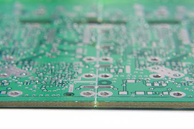
Bare Board Test
Bare board testing is when a correct PCB service provider. Thankfully, there are various PCB manufacturing firm tests the continuity and isolation of electronic connections on an empty PCB board before attaching essential components such as ICs. Continuity PCB testing involves verification to ensure that there aren’t open points in the circuit. On the other hand, do isolation testing to verify that you meet the required resistances between two separate electrical connections. The idea behind bare board testing is to ensure that the PCBs circuit part is correct. Among other things, bare board testing is essential since it can save manufacturing firms money and time, thereby avoiding issues to do with repair, field testing, and maintenance costs.

Assembly Level Test
When it comes to Printed Circuit Board Assembly, an assembly level test is essential. The assembly level test is critical for checking the printed circuit board’s functionality after the completion of the meeting. These tests can be done manually or by the use of automated test equipment. It is important to note that this equipment is a little bit expensive as Printed Circuit Board Assembly level tests require several testing devices such as Automated X-ray Inspection and Automated Optical Inspection devices, to mention but a few.

Online Test
Online tests, also referred to as automated tests for Printed Circuit Board Assembly, are completed after the manufacturing process is complete. Here, printed circuit boards go under inspection using a flying probe or an adapter E-Test for a more extensive series. Several online test equipment and software can you can use to carry out printed circuit boards’ online tests. Among other essential written circuit board tests, online PCB tests are some of the most vital tests that published circuit boards have to undergo before being rolled out to the market.

On-line testing of FICT Without Fixtures
Also referred to as the flying probe test, the fixtureless in-circuit test (FICT) is an ICT that works without custom fixtures, thereby reducing the overall test costs. First introduced way back in 1986, a fixtureless in-circuit test employs a simple installation that holds the board as the test pins move around and test the relevant points on the board. It does this through a software-controlled type of program. Since the introduction of FICT, it has gone ahead to gain widespread use, especially across the electronics manufacturing industry, based on its versatility. Even though FICT can adapt to new boards cost-effectively and with a lot of ease, it tends to be slower. Therefore, this makes it one of the best testing methods, especially for small prototype PCB assembly and testing, but somewhat less effective for large-scale printed circuit board production.
Functional Circuit Test
Functional testing is the last gatekeeper in the PCB manufacturing plan. The functional testing provides either a go or a no-go choice on finished printed circuit boards. By the time a manufacturer arrives at the functional tester, they’ll be testing the product’s functionality. Here, they won’t be testing as to whether the board is good or bad.
They don’t want to see if the solder is present or missing or if the component is out of tolerance. A functional test is done and looks at the overall product. A practical analysis ensures that the assembly is in the right manner and that everything works together. It is important to note that functional testing is not ideal for early prototypes because it does not identify details on what is wrong with the product. Generally, printed circuit board functional circuit tests look at the product’s functionality as a whole and then grade it as a pass or fail.

Boundary Scan Test
Boundary-scan tests are also some of the most important criteria to perform before you place a printed circuit board on the shelves for purchase. This type of analysis looks at printed circuit board wire lines and is a preferred means of testing integrated circuits, especially when it becomes impossible to reach all the PCB nodes. When it comes to boundary-scan tests, cells get placed in the silicon leads to the external pins to test a printed circuit board functionality.
A differentiating quality regarding this type of test is that it can assess the board without reaching or touching a board’s entire nodes. This is essential, especially when evaluating integrated circuits containing high density and multiple layers with such types of printed circuit boards becoming prevalent lately. Boundary-scan tests are standard in field service for purposes of detecting defects across functioning systems.

JTAG Test
Testing remains to be essential, especially when it comes to the production of high-quality printed circuit boards. Among other types of tests, the JTAG (Joint Test Action Group) test is also essential for the manufacture of printed circuit boards. Most people regard the JTAG test as the industry-standard test whose purpose is to verify designs and test printed circuit boards (PCB) after the manufacturing process is complete. JTAG tests are essential as they assist printed circuit board manufacturing in three ways: it is highly cost-effective, it saves a PCB manufacturer’s time, and strengthens the quality of their products.

X-ray Fluorescence Transmission
The X-ray fluorescence transmission is a test process used in viewing the internal construction of a printed circuit board, including vias and layers. X-ray fluorescence transmission is also a standard test in seeing the inside components of a printed circuit board to verify device authenticity. During such inspections, an X-ray electrician can locate or find defects early during the process of PCB manufacture by viewing internal traces, barrels, and solders connections. X-ray fluorescence transmission tests check elements that are usually hidden from view, though such tests need to be conducted by trained and highly experienced operators.

X-ray lamination system
Closely related to X-ray fluorescence transmission, the x-ray lamination system is another critical test method that works by generating a focal plane of a horizontal area through the process of scanning or an x-ray detector synchronously spinning.
X-ray lamination systems are used to verify the mechanical integrity of printed circuit boards. It identifies other errors such as missing solder joints, solder bridges, inadequate wetting, and misalignments. Even though the x-ray lamination system is costly. It is essential as it significantly shortens the time or reworks and searching.
Lon Contamination Test
More than 25% of printed circuit board failures happen because of ionic contamination. Ionic contamination may bring about catastrophic PCB failure, which brings about financial losses for a PCB fabricator. Also referred to as resistivity of the solvent extract (ROSE) test. The ionic contamination test effectively detects ionic tissues that remain from the process of manufacture and soldering. By testing a PCB for ionic cleanliness, manufacturers can avoid issues to do with conformal coatings.
Chemical Resistance Test of Solder Mask
Soldermask is highly prevalent in the manufacture of printed circuit boards. The main aim of the solder mask’s chemical resistance test is to identify or instead examine a solder mask’s chemical resistance. Conducting chemical analyses of the solder mask is not a complicated process as such. All you have to do is drip the sample’s surface with dichloromethane. Then wipe the dichloromethane with a white cotton cloth. After that, you need to check whether the fabric is dyed and whether the solder resist is completely dissolved.

Hardness Test of Solder Mask
This type of analysis aims to examine the hardness of a printed circuit board’s solder mask. To do this, you need to put the PCB on a clean flat surface and use the standard test pencil to scratch the entire board. Lastly, you’ll have to record the minimum hardness of the pen. The minimum hardness needs to be above 6H.
Conclusion
Regardless of the type of method you choose to use, printed circuit board testing is a vital step during PCB design. helping you to avoid unnecessary costs and time by ensuring that you avoid bugs way before they affect the entire production. Again, to successfully run printed circuit board tests, you need a reputable supplier that you can trust. WellPCB can help. At WellPCB provide you with both small and large scale production services to speed up your testing needs. With no hidden fees and incredible reliability, you can rely on us for quality PCB tests.