Contents
What Is a Silicon Circuit Board?
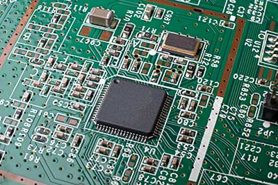
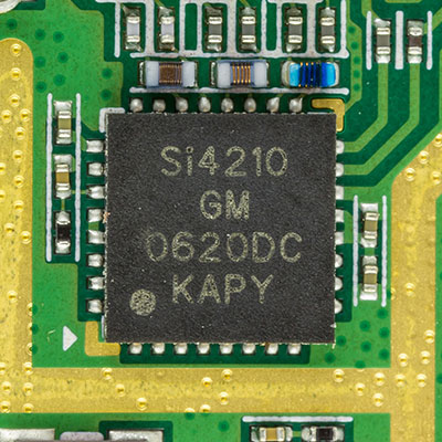
SiCBs or silicon circuit boards look like standard PCBs. However, the difference between both boards is that the former uses a silicon substrate while the latter uses FR4.
Also, you can create silicon circuit boards in any silicon wafer foundry. All you need to do is use the front-end-of-the-line or back-end-of-the-line processing—based on your foundry.
Further, the sizes of SiCBs lie between printed circuit boards and integrated circuit elements. So, since the PCB has a dimension of 10 x 10 inches, a standard SiCB is 2 x 3 inches, and ICs are half of an inch on each side.
In addition, you can change the design of a standard FR4 PCB into a small SiCB (less than one-quarter the size of the PCB). All you need to do is remove the package’s dice and decrease the trace sizes.
Can you add an HPC (high-performance computing) design to the SiCB? Yes, you can. But you have to add the following components:
- Clock drivers/ chip-scale-package oscillator
- I/O connectors
- Memory dice (8)
- CPU die
- Large FPGA dice (4)
- Bypass capacitors
Your circuit design should have a 60mm x 70mm dimension and a thickness of less than 3mm with these components. But you can add more millimeters for a heat sink.
Features and Benefits of the Silicon Circuit Board
The silicon circuit board has the following features and benefits:
Signaling
Due to the shorter distance on SiCBs compared to a standard PCB, it has a faster signaling speed. So, removing the circuit board’s package helps to reduce its capacitance and parasitic inductance.
Also, these circuit boards feature relatively small wires of about 2 x 8 microns.
Hence, they can be resistive, perfect for a signaling environment. Consequently, you may not need to terminate transmission lines, decreasing radiated energy and EMI.
In addition, you can do high-speed signaling via a TSV. But ensure that it doesn’t exceed 100 microns because it may cost a lot of signal integrity.
Low Power
If you compare the standard PCB to the SiCB, you’ll notice that the latter has reduced cooling needs. And that’s because there’s a significant reduction in the I/O power requirements.
Interestingly, you may see a circuit board with I/O power lower than 10% of the packaged part I/O power. Also, you may notice more decrease in the I/O power if you design a custom I/O for the SiCB electrical connections.
Reliability
This device has enhanced reliability because the temperature coefficients on the silicon circuit board and bare silicon dice match. So, you can use this circuit pattern for HPC without worrying about system failure.
Another advantage of using a SiCB-based system is its few parts. Hence, you can quickly repair or rework it compared to the FR4-based system.
Links Of Supply Chain
No doubt, the SiCB design, rework, test, parts, and manufacturing have available supply chain links. But the chain isn’t workable because they aren’t connected. But these links will join as technology advances.

How to Design and Build a SiCB
Here are the steps you need to build a silicon circuit board:
Step 1 – Start with The Design
To begin the SiCB design, you can opt for either an IC layout tool or a PCB layout tool. Further, it’s vital to note that none of these tools are appropriate, but they’ll work perfectly.
How? PCB tools are ideal for routing, not dimensions below a micron.
And they don’t produce IC output files (GDSII).
On the other hand, IC design tools focus more on the area. However, it lacks both ease of use and routing performance.
Step 2 – Get the Tested Parts
You can quickly get bare-dice datasheets from factories or online. But it’s vital to ensure that the parts undergo complete testing in die form.
Step 3 – Build the SiCB
You can build the SiCBs with semiconductor IC fabrication technology. However, the issue is that the foundries may have reticle limitations. And you may end up with only small SiCBs or silicon interposers.
So, if you want a giant silicon circuit board, opt for reticle stitching. Alternatively, you can consider older fabs because they complete silicon wafer masking.
If you’re fabricating an interposer, you can do copper thickness metallization that’s about 2 microns thick. However, this process isn’t ideal for SiCBs because their minimum appropriate size is approximately 5 microns.
In addition, you can add different substrate materials like glass, organics, and ceramic substrates.
Step 4 – Assemble the Circuit Board
Assemble the SiCBs by using high-end PCB assembly houses.
To do so, you’ll need an automated pick-and-place machine with excellent ESD control.
Then, follow the surface mount design rules for the part assembly and work with pad pitches of about 30 to 40.
In addition, since there’s a similar temperature between the SiCB and the die, you don’t need a bare die underfill because of the decreased mechanical stress/thermal stress.
Step 5 – Test and Rework
In this step, you can test your assembled SiCBs by combining wafer probing test fixtures, self-test, modified package, and flying probe test. Also, if you need to replace components, use PCB rework methods.
Rounding Up
Silicon circuit boards are similar to the standard PCBs but with a silicon substrate. Plus, they allow a pad pitch of about 30 to 40 microns.
Also, this device comes with intended components like the stacked 3D die and bare die. And you can make them with specific processing based on the foundry. Further, due to the unique features of this device, it can pass for an HPC design. Do you plan on building a silicon PCB? Or do you want to get the best one for your project? Please feel free to contact us.