Contents
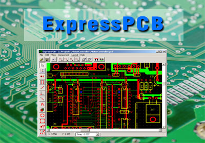
ExpressPCB
1.1 What Is It?
ExpressPCB is CAD software for printed circuit board (PCB) layouts. The CAD is divided into the more helpful category:
• ExpressSCH is used to design the schematics. Both Classic and downloads include the same schematic design software (ExpressSCH). You don’t want to download extra things, and the essential thing is you also don’t need to worry about learning it
• ExpressPCB to create a PCB design. It is linked to the schematic. Expresspcb.com owns the output file. They will provide the Gerber files for a fee.
• ExpressPCB Classic is the original layer software you are already familiar with. This software is beneficial when making a 2- or 4-layer PCB. Schematic linking allows easy verification of your layout design. Classic designs can be easily changed into plus designs.
• ExpressPCB plus Our new layout software has a modern look and offers additional features and capabilities for your two—and four-layer PCB designs. The critical thing to note is that this does not currently have a schematic linking to the layout.
It is straightforward and useful software.
It provides many facilities to the user, but it has limited libraries. These little libraries may not affect their efficiency. This limited version has all of the features required for the basic and advanced features.
Also, these limited libraries allow you to build your customized library and components.
ExpressPCB is used to assemble the components of the basic design. Then, you can quickly change the design into a schematic drawing and then into a PCB design layout.
ExpressPCB is a very flexible software that can efficiently fulfill your desired projects.
1.2 Charge Or Free?
It is straightforward software for beginners, so you can easily download the accessible version of that software. The latest version, 7.6.0, is available.
The CAD files are in propriety format, but ExpressPCB can also supply you with the Gerber format.
The charges for Gerber files (so far) are $60. You can order it through the mail and get that facility. The costs are added to the same credit card on which you placed the board order.
ExpressPCB Tutorial
2.1 ExpressPCB Free DownloadRegarding
As far as the download procedure, you can easily download the latest version from expresspcb.com directly.
On this website, the latest versions are present. You have to download the understanding of your desire.
2.2 ExpressPCB Tutorial
As you know, this software is straightforward to use and learn for beginners. This tutorial will help you out with more details, and at the end of this tutorial, you can easily design your PCB. In ExpressPCB, there are two stages of designing.
1. ExpressSCH
2. ExpressPCB
You have to follow the steps that are listed below to create a PCB from hand drawing to the PCB layout:
• Select the circuit diagram which is already been tested on the breadboard.
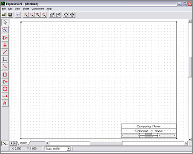
• Open the ExpressSCH for fresh design. When you start the system, a dialog box is also open; this will help you withae general overview of the tools. Once you begin to do so, close the dialog box and view the new schematics.
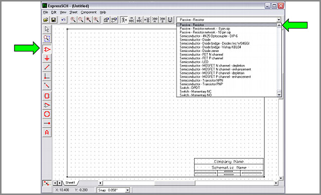
• After that, place the desired components by clicking the op-amp-like symbol in the left-hand toolbar. For example, suppose I have to put the resistors and diode in the schematic; you can place these components by searching the component names in the text box.
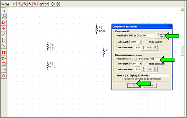
• When you place the desired components, you must give them a unique identification. Right-click on each feature and choose the component properties.
First, select the auto-assign part ID. This will assign the name according to the placing order.
Then, set the value of each component by selecting the part name and hitting OK.
In my case, I placed the four resistors and named them as shown.
• You can quickly rotate the components; right-click on an element, select the rotate feature, and turn it as you want.
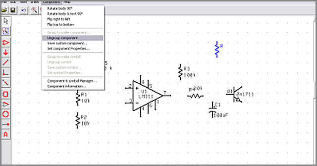
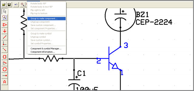
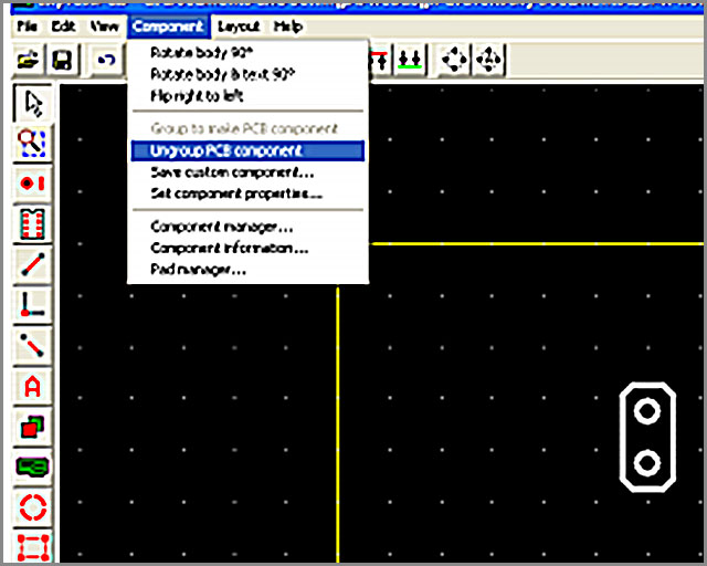
• Sometimes, some components are unavailable in the directory; for example, I have to use a photo-resistor in my circuit diagram, but it is unavailable. I have to place the passive resistors from the previous method. Go to the Selection tool (the arrow), choose the resistor, go to the component menu at the top, and select the ungroup component.
- Draw a circle around the resistor by selecting the circle option in the tool menu.
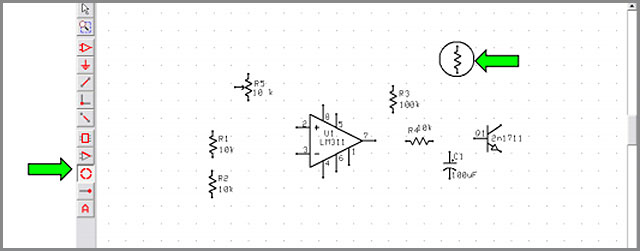
- Select the whole object (using the arrow tool), and choose Component -> Group to make the component.
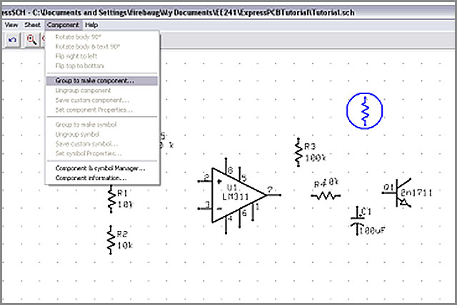
- After building your component, you can also save it by selecting it and choosing to save it as a custom component. A dialog box appears for the unique name. For example, suppose you build a photoresistor, so keep this as a name. Then, similarly, give it a unique ID and value from the old procedure.
- Now, we need to add the power and the ground. Let’s start with the ground command. Go to the toolbar’s symbol/signal label, open the text bar, and choose the power-ground option. Moreover, place as many rounds as you want.
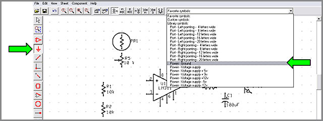
• Now, for the power supply, do it again, but this time, the name power voltage is equal to the 5V power supply.
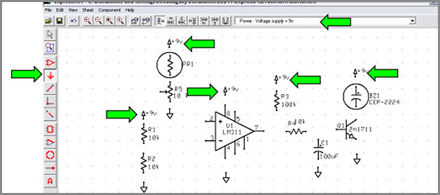
• The last stage of the circuit is to connect it with the battery; you have to write the misc-battery in the text box, place it, and then give it a unique name and unique ID.
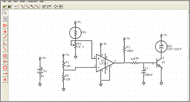
After that, wire your circuit by choosing the option wire from the toolbar, left-click will start the wiring, and right-click will end the wiring, and in this manner, your course will be completed like this. In my case, the final schematic looked like this:
- The next step is to save your file using save as with a unique name and path.
- Now check your file for netlist error using file and go to the check error for netlist error.
- Suppose you are using BJTs in your circuit diagram and you did not specify the pins of the BJT. Then, you will probably get an error message.
- So you have to do is hit the cancel button on that message, and as the message suggested, select that part of the component. Then, go to the component and choose the ungroup component. After that, double-click the emitter, base, and collector one by one and set their names 1, 2, and 3, respectively.
- Afterward, select the whole component again, go to the menu, select a component, choose group the component, and then set their part name and ID part.
- Now again check your file via netlist error, now this time you will not get any error.
- You may face one more error if you don’t skip#28. This error probably occurs when any wire is not connected or the snap-to-grid function is not enabled. Hit continue and then remove this error to disable the snap-to-grid option. Select the errant lines and move them into the correct position. Do this until you get an error-free message.
- When the netlist error shows that the schematics are clear, you will run the program, save the file, and print your schematic diagram.
- The above discussion is related to the schematic diagram in the ExpressSCH. Now, we will discuss the ExpressPCB.
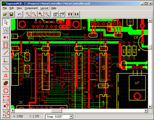
2.3 Creating The Layout In ExpressPCB
- Open the ExpressPCB. When you start the file, a dialog box appears. It contains two links. If you have time, read them; they are very instructive. Otherwise, hit OK and start the file.
- The next step is to go to the file and select the new file. Now, again, a dialog box opens where you have to set the dimensions of the board. By default, it is 0.056 round via with 0.029 holes. That is the maximum default size, but you can change it as per your requirements.
- Now, you have to place the components in the plane. Select the IC-like icon from the toolbar and the pull-down menu to choose the components. Double-click the components to select their properties.
- If you need to place a transistor, select the same icon and place the Dip-8 pin. For capacitors, write their cap and then assign the name and part IDs.
- The same procedure is followed. If any of the components are not present in the layout, you can draw them yourself.
- Place the similar component as you did before going to the component and choose the ungroup PCB component.
- Now, draw the circle in my case because I am drawing a photo-resistor and set the radius of the circle and the line width.
- Then again, select the whole part, go to the component, and select the group to make the PCB component.
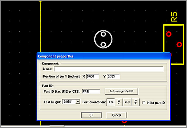
- Now, it’s time to assign the unique name and ID, so double-click on the component and set these parameters.
- To use this component again, save this as a custom component.
- Repeat this for different components as you want to make parts.
- For placing the grounds and power into the circuit, wne have to choose the FILLED PLANES option from the toolbar and then select then click on it to select the layer.
- Then, draw a horizontal line and drag it squarely.
- Then, select the place traces.
- When you draw the traces, an isolated path is created. This path separates the ground from the power.
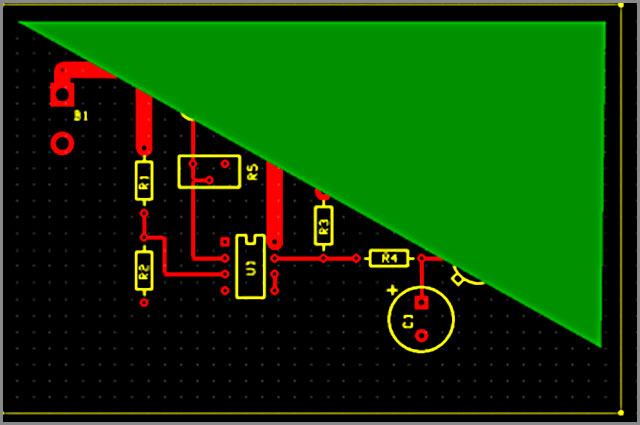
• Continue down to the bottom right corner and then to the bottom left corner. Then, right-click to end the box. Your display should now look like this:
- When the filled plane is added to the circuit, you can change the shape of the plane.
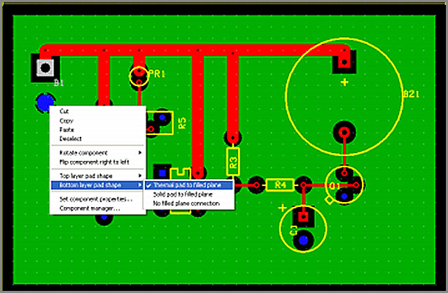
- You can connect the pads using thermal or solid shapes.
- Connect the plane to the pad by right-clicking on the pad.
- When you connect the plane with the pad, you have to select the plane type, and the pad type with it is a solid/thermal plane and solid/thermal pad.
- There may be an area where you do not want a filled plane. To keep that area out of the filled plane, select this icon and then choose the area that keeps it out of the plane from the top toolbar.
- In a similar manner, draw a square in the area where you do not want a filled plane, and this time, the area will show with the dotted lines.
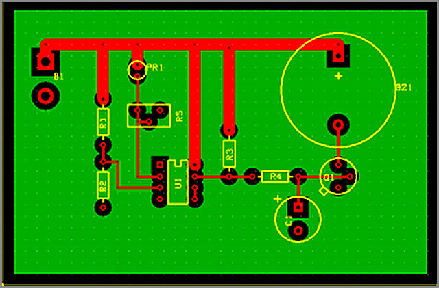
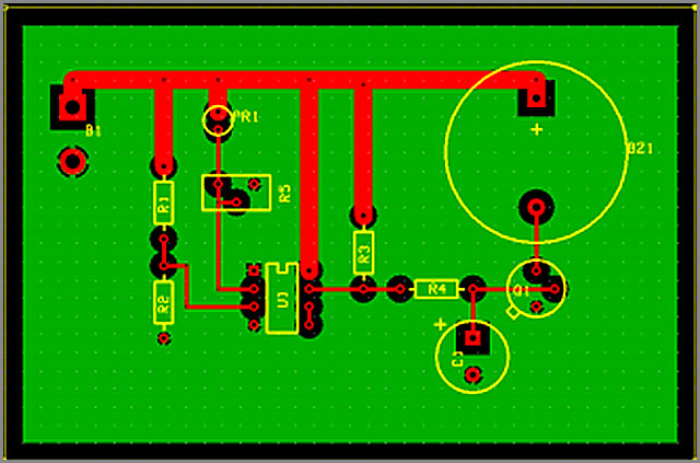
• Repeat this for all of the pads; now your layout should look like this:
- By using ExpressPCB, you can also create multiple layers.
- First, you have to set the number of copper layers. You can quickly select the layers from the layout menu. If you are choosing the four layers, then this will add two inner layers the first one is the ground plane, and the other one is the power plane. These layers are filled with the copper plane that will improve the noise immunity of the circuit.
- After you complete your layout, the ExpressPCB program tells you exactly how much it costs to make the boards.
- Now you can take the print out of your manufacturing of PCBs, there are high chances of layout failures, which can go a long way into negatively affecting the final product’s functionality. There are several PCB layouts.
- These are some precautions that we have to take while making the tracks (making connections between the components):
► Make certain tracks do not have bends less than 100 degrees.
► The way does not touch each other. It may fail devices.
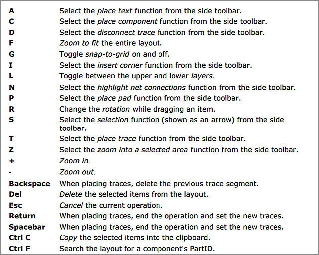
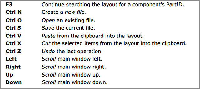
- Some of the short keys are given below:
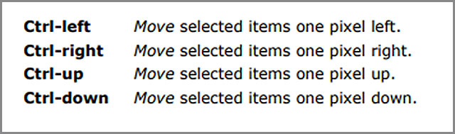
• After making the layouts, you can delete, move, copy, and rotate the component.

ExpressPCB To Gerber
Yes, ExpressPCB files can be converted into Gerber files easily and quickly. You have to place your order of Gerber files on the online store and enter your ExpressPCB order number.
You can quickly generate the Gerber files using your order number’s original PCB design file. Also, I will email the Gerber files back to you as an attachment.
You will receive these files:
- Silkscreen layer
- Solder paste and mask layer
- The top and bottom copper layer
- Drill files
- The layers design also includes two inner layers
First, we will discuss how you will change the ExpressPCB file to PDF. The other way is first you convert the ExpressPCB file to PDF, and the PDF will be converted into the Gerber file. The steps are given below:
- Open the PDF file and select the PCB manufacturer. The process becomes more hectic. They will design the PCB layout.
- Go to the file option and select the print option. A dialog box will open. As you know, the PCB layout contains two layers: the copper layer and the silk layer. First, we will convert the copper layer.
- When the dialog box is open, you have to set these parameters: PRINTER: CutePDF writer and LAYERS TO PRINT: check the top copper layer, uncheck the last option print in color, and hit OK.
- After that, save the file; the first layer is converted to PDF.
- The silk layer is also converted into a PDF file similarly by only changing some settings, i.ne., layers TO PRINT: check the silkscreen pads and text on the top layer. So hit ok and again save your file.
Now, we have to convert these PDF files to Gerber files. The steps are straightforward:
- First, open the Gerber software
- Go to the file, select the option import, and then choose from the postscript/PDF.
- A dialog box is open when you select it
- Select PCB_sample there and hit OK
- Another dialog box is free from that dialog box. Change these parameters: MAP LAYER: a separate color per layer, and press next.
- After downloading, your PDF is converted to a PDF file.
- You can now change things as you want.
Comments On ExpressPCB
As you ask about the ExpressPCB from the user, they mostly say that the software is easy to use, very friendly, and has high-quality files, but they have insufficient mechanical support.
The most significant advantage of this software is the format is etiquette, and ExpressPCB can accept only this.
They offer very easy shipment and straightforward payment. You can pay your price by clicking just a few buttons, and the ship will be on its way.
It is evident that a thing that has a plus point where negative points also exist.
Other than that, the price is acceptable and easy to achieve.
So, this software also has some negative aspects. They have cut themselves off from the rest of the ecosystem in that you can’t use their software with another fab or vice versa, and they are paranoid about people using their files for other stuff.
You can’t easily version control or do your DRC on their format, although third-party tools are available that show that someone must have reverse-engineered the file format. Also, some of the quick-turn boards are not RoHS.
Also, you cannot change the hole size by the default settings. However, this software is hard to be after all of those negative points.
Conclusion
At the end of this discussion, you are now well aware of the PCB software ExpressPCB and its usage of this software.
From now on, you can select the best PCB software for your project, which will provide you with the highest-quality results and long-lasting effects.
WellPCB is the place to get the best PCB manufacturing and assembling services. Our expert team will give your project the best results and deliver it within a short time.
For more information on PCB materials and other topics of interest, contact our support team at [email protected]et.


