Contents
Chapter 1: PCB Design and Layout
1.1 PCB Design Software
The PCB production process begins with design, and it’s crucial to select the right design software. This choice helps you:
- Route traces properly
- Design vias as needed
- Ensure the layout meets design requirements (such as trace clearance and width)
- And much more
Considering these factors is essential for choosing the right software for your project.
Feature Set
The software should offer features like a comprehensive component library, which can reduce design time by eliminating the need to import external parts. It should also support multiple layers to facilitate complex PCB designs, board simulation to identify potential issues (such as components placed too close together), design rule checking, and 3D modeling with zoom capabilities for both bird’s eye and close-up views of all features.
With the right software, the PCB production process becomes much smoother, ensuring accuracy and efficiency in bringing your designs to life.
Overall, the more features the software has, the more powerful and capable it is for handling different PCB design projects. Some options worth checking out include Altium Designer, Autodesk Eagle, and DipTrace.
Ease of Use
The two factors to consider here are an intuitive user interface and a short learning curve so that you can get the ball rolling in a short time. But don’t sacrifice features for a short learning curve. Always place the feature set before ease of use.
Integration and Compatibility
Check the design software’s capability to integrate with other CAD tools, as well as its support for different file formats. The broader its integration and compatibility, the smoother your workflow will be.
Cost
The last factor is cost. Advanced PCB design software can be expensive, especially when you factor in multi-user licenses and add-ons. But there are cheaper alternatives, although some might not be of the best quality. So, compare the features and quality first, then narrow down your list using the cost factor. You can use this guide as a start.

1.2 PCB Layout Considerations
Board Size and Component Placement
First, depending on the purpose of the PCB you are designing, you must consider the size and shape of the board.
The board is a primary component of the PCB because it holds all the other parts. Factors determining the size and shape of the PCB include the functionality and size of the destination product.
For example, wearable products such as activity trackers require way smaller PCBs than televisions.
As for component placement, consider the manufacturing of the PCB because that is the end goal. For instance, similar components, such as transistors, should face the same direction when placed for easier installation and inspection by the manufacturer.
Keep in mind the size and height of each component. Some components will be larger than others, which may result in uneven bumps on the circuit board when placed next to each other.
Some taller details may block shorter elements, and when the board is passed through the soldering oven to engrave the parts onto the board, it may return with poorly connected solder joints.
Always consider the height and width of components on the board – details of similar dimensions can be placed towards one side, ensuring the soldering wave reaches the smaller parts without being blocked.
Also, leave space for routing. If you place components too close together, you will run out of reach when you start routing. Integrated circuits, for example, have lots of pins to be connected around the board. To prevent running out of space and jumping over your design layout again, give enough room for components that require lots of pins to be connected to make the process easy.
Signal Routing Techniques
Consider these techniques when routing the traces.
- Use Auto Routing Judiciously: Auto routing sometimes only considers the intricate nuances of specific PCBs, so manually oversee this process to prevent power, signal integrity, or ground issues later.
- Use High-Speed Signal Routing to Reduce Interference: High-speed routing can incorporate things like placing these traces above a solid ground plane, keeping trace widths even, using vias to avoid hot spots, and avoiding bending traces at 90° (135° is better). Look out for impedance when routing high-speed signal lines.
- Implement Daisy Chain Routing for Identical Components: When routing buses to connect similar components, such as memory module RAM chips, daisy chain routing provides a more organized, less cluttered routing design than routing to each part individually. But you have to account for the signal delay when the signal passes through each component chain. This is more significant in high-speed designs.
- Use Dedicated Power and Ground Planes: These planes in multilayer PCB designs ensure components receive reliable power, provide a stable reference plane, and shield the signal lines from EMI.
Establishing Design Rules and Guidelines
Remember to establish the ERC (Electrical Rules Check) and DRC (Design Rules Check) guidelines for quality control purposes during design to ensure the manufactured board is functional and error-free. They include defining physical requirements like trace and gap widths, via-hole selection for different nets, and high-speed electrical requirements to automate the PCB layout review to validate the layout.
Set these rules before beginning the design and layout processes, and run them throughout the design process to help identify and rectify potential issues early on. Running the rules at the end of the design process can highlight multiple errors that require tons of rework, which will waste time.
1.3 Stack-Up and Material Selection
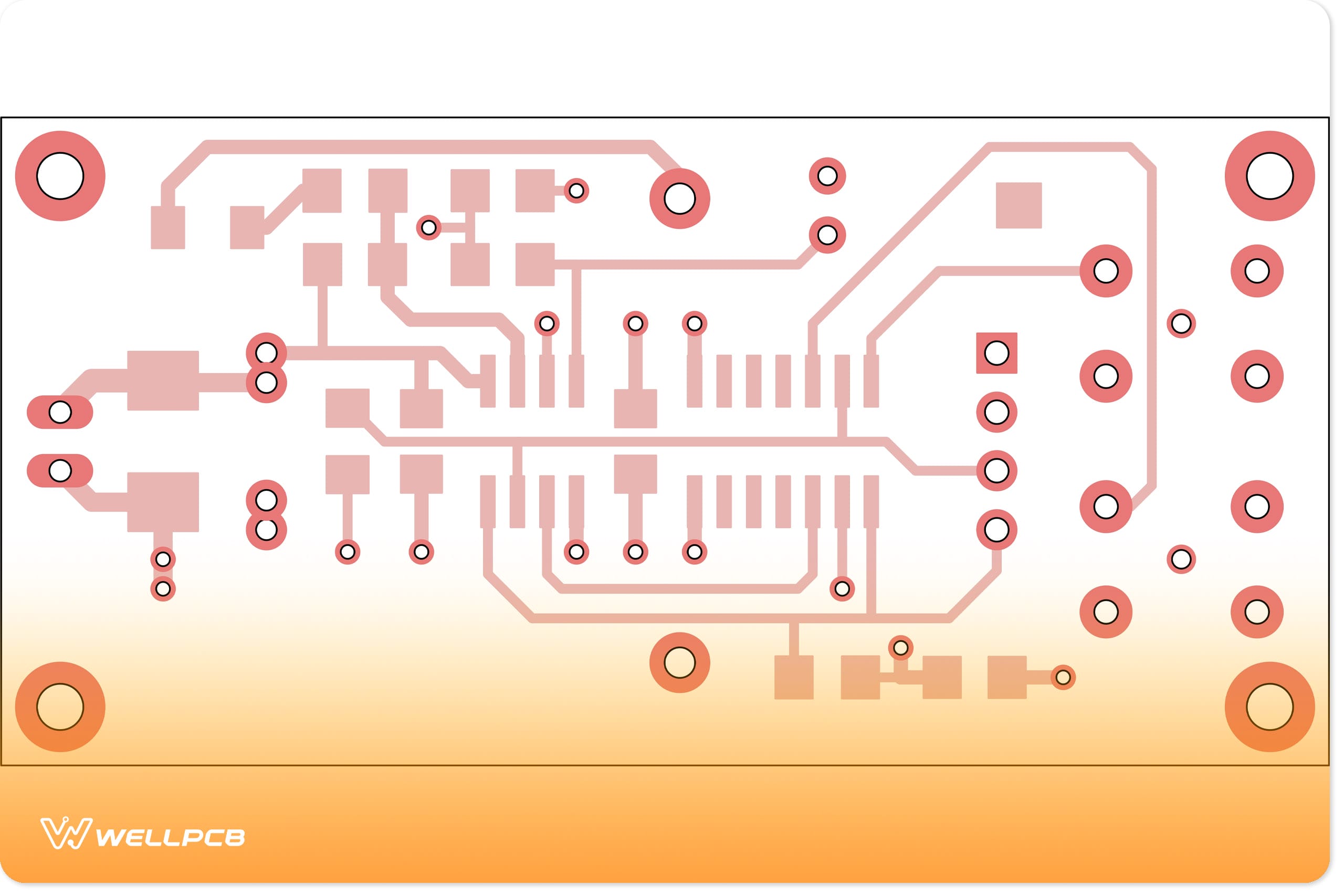
PCB stack-up forms the foundation of the entire PCB. It involves placing insulating and copper layers and laminating them with an adhesive. The stack comprises the various layers within the PCB and allows you to establish the characteristic impedances at each layer. But the more layers the PCB has, the costlier it becomes.
The top layer is the silkscreen that adds other indicators, such as letters and symbols, to the board, while the bottom layer is the substrate/dielectric (usually FR4), which gives the board its rigidity and thickness.
The ones in between are the copper layer for conductivity and the solder mask, which gives the PCB its distinctive green color and protects the copper from oxidation.
Optimal multilayer stacking cuts off external noise, enhances the design’s electromagnetic compatibility, keeps the cost within budget, and ensures efficiency in the manufacturing technique.
Material Selection Based on Thermal Performance and Cost
The material that usually varies depending on the application, thermal performance, and cost is the dielectric. FR4 is the most commonly used one because it is relatively cheap. However, since it is a fiberglass material, it isn’t a good conductor of heat.
For circuits with hot components like LEDs, metal is the better alternative because it dissipates heat quickly while providing structural strength as well. Metal also has a higher glass transition temperature, so it won’t deform when temperatures rise. The most commonly used one is aluminum.
However, metal is also electrically conductive, so there must be an insulation layer between the substrate and the circuit, which reduces heat dissipation. So, another alternative for PCBs with extremely hot components is ceramic. But ceramic is very expensive, so metal is the preferred option.
| Material | Composition | Thermal Conductivity |
| FR4 | Fiberglass and Epoxy | 0.25W/mK |
| Rogers | Fluoropolymers | 0.7–1.7W/mK |
| Metal | Aluminum or Copper | 150–400W/mK |
| Ceramic | Alumina or Aluminum Nitride | 25–250W/mK |
1.4 Vias and Thermal Management
Via Types and their Applications
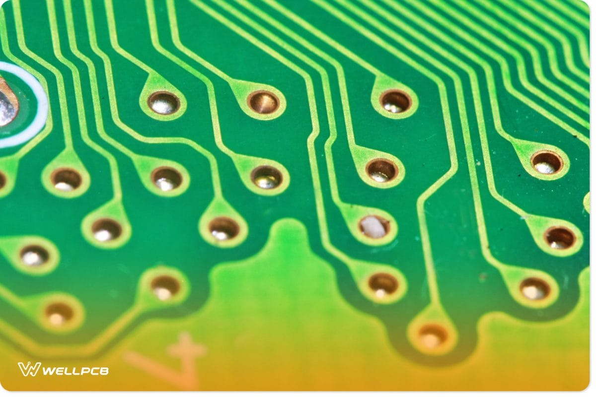
A PCB via-hole allows interconnections between different layers of the board. Vias may join traces, pads, and other conductive elements and provide the path for electrical and thermal energy moving from one layer to another.
Since we drill holes through the board to create the vias, you must consider each hole’s placement and size in relation to the other PCB components.
Ensure all the vias on the board are the same size to improve efficiency in the manufacturing process.
There are three basic types of vias: through vias, blind vias, and buried vias. Through vias connect two visible exterior layers. But blind vias connect a visible outer layer with an invisible interior layer, while buried vias connect two hidden interior layers.
Other vias include thermal vias for transferring heat from the top layer to the bottom or internal layers and tented vias enclosed with solder masks to prevent electrical and thermal components leakage.
Be sure to discuss the capabilities of the via types you intend to use with your PCB manufacturer because different vias have different heat and current-carrying capacities.
Managing Thermal Issues in PCB Design
Thermal issues affect larger circuit boards with higher density and excessive processing speeds. To avoid such problems, your PCB must allow heat to dissipate.
During the material selection, identify components generating a lot of heat and find ways of diverting heat from them. The surface space around parts quickly becoming hot is a crucial layout design consideration because they’ll need space to cool off.
You may consider including heat sinks, cooling fans, and thermal reliefs.
Some places to add thermal reserves include through-hole vias to slow the heat sinking rating through the PCB layers.
Chapter 2: Generating Gerber Files
2.1 Understanding Gerber Files
A Gerber file contains information that guides the production of a PCB. As you might have observed, the Gerber file format is a de facto standard that defines 2D binary images using open ASCII vector format.
Modern Gerber files may also include metadata (data about other constituting data within a file) like solder mask, legend/silk, and number of copper layers, among other relevant printing information.
PCBs are made from Gerber 274-X data and NC drill files.
Each Gerber file corresponds to one layer in the physical board – the component overlay, top signal layer, bottom signal layer, solder masking layers, inner layers, etc.
This file format is important because, in 2015, UCAMCO estimated that about nine in every ten PCB productions are presented in Gerber form.
Here’s how to generate Gerber files using Eagle 3.55 and Altium Designer.
Eagle 3.55
First, you’ll need to download another definition file: the CAM file. EAGLE provides this CAM job file, so to create your Gerber file easily for a 2-layer board, first download these files:
- eagle to gerber1.doc;(39.5 KB)
- Eagle user brochure.pdf; (289 KB)
- IPC-a-600.pdf(1.50 MB)
After that, follow these steps.
- Load your board on the screen.
To do this from the Eagle Control Panel, click on File/Open/Board and select the board you will use.
- Click on the Icon on the top Toolbar that says ULP.
When the dialog box appears, select the ULP file called DRILLCFG.ULP from the ULP directory. In a matter of seconds, on the command line, you will notice a message saying ULP has finished.
- Now click on the Icon that stands for the CAM Processor.
This will load the CAM Processor Screen. From this screen, click on File/Open/Job (when asked to save “Modified Job” reply NO) and select the CAM job called GERBER.CAM from the CAM directory and click OK.
- Now click on the button that says Process Job.
This will prompt you with two messages. The first message will be “Delete the $$$ file after process.” This is a dummy file that EAGLE creates. Click OK. The second message will be “More than one signal layer Active.” Click OK to this message as well. Depending on the size and complexity of the board, the entire process will take a few minutes or hours.
- When the CAM Processor stops all processes, it has finished.
This process created several files that will have the same name as your board with different extensions:
- .WHL Aperture Wheel File.PLC Silk Screen Component side
- .CMP Copper Component side.STC Solder Stop mask Component side
- .SOL Copper Solder side.STS Solder Stop mask Solder side
Zip them and send them to your PCB Manufacturer.
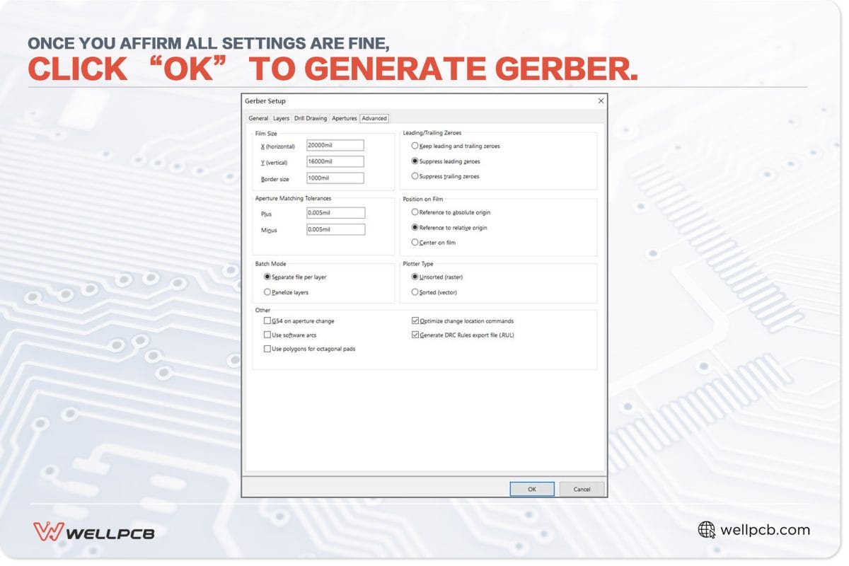
Altium Designer
- Select “File” menu, >> “Fabrication Outputs” >> “Gerber files”

- In the dialog box, specify the parameters for measuring the PCB.

- Select the layers: For a 2-layer board, uncheck layers G1, G2, and G3 ….
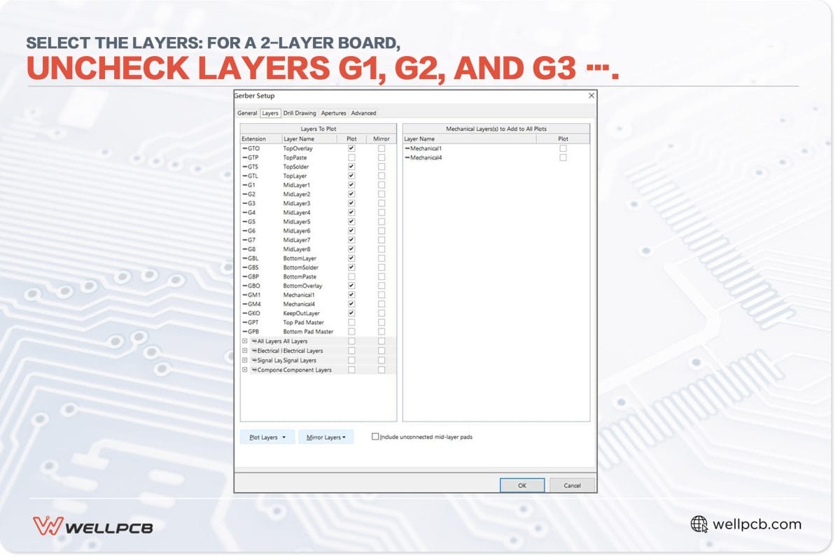
- Check the Embedded Apertures

- Once you affirm all settings are fine, click “OK” to generate Gerber.
2.2 File Extensions and Viewer Tools
Gerber files are often associated with the file extension “.gbr” or “GBR.” However, other extensions like “.GBX,” “.Top,” and “.BOT” are also used to define Gerber files.
And even then, the “.gbr” extension does not exclusively apply to PCB Gerber files. Sometimes this extension is still used by other image editing software applications like GIMP to represent the applications’ image brush files.
On the other hand, a Gerber file viewer is software that allows you to view the contents of a Gerber file. Currently, there are a variety of Gerber viewing tools on the market.
Some of these tools work by installation (much like traditional software applications), but most work online without being installed on one’s computer. They allow you to upload files and view the Garber files online.
The key features to consider when choosing Gerber file viewers include:
- File format support: An ideal Gerber file viewer should be able to support popular modern file types like HPGL/HPGL-2 and Excellon, among others.
- Support precision in viewing: Good Gerber viewers should also include features for zooming and precision measurements so that users can easily check through circuits and rectify errors.
- Broad printer compatibility: Gerber file viewers should also be compatible with various printers. Besides, it should also give room for various printing options for various printers.
Best Gerber Viewer Tools
Of all the several Gerber viewing tools available in the market, the following three tools are currently the top-rated tools for viewing Gerber files:
The Online Gerber Viewer
It is compatible with Gerber274X and Excellon 1 and 2 file formats. This tool also allows you to zoom in whenever you need to check your boards for design errors.

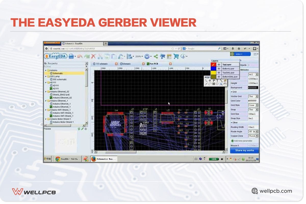
The EasyEDA Gerber Viewer
EasyEDA is an awesome online Gerber viewer with nearly all the features of the Online Gerber tool. But unlike the Online Gerber, EasyEDA allows you to view the layers of an uploaded/imported PCB, zoom through, and choose the color for the PCBs.
It also has some statistical features that allow you to compare the shapes and sizes of the holes and dimensions of the board. Once you have done this, EasyEDA will offer you the option of sharing your files using a URL.
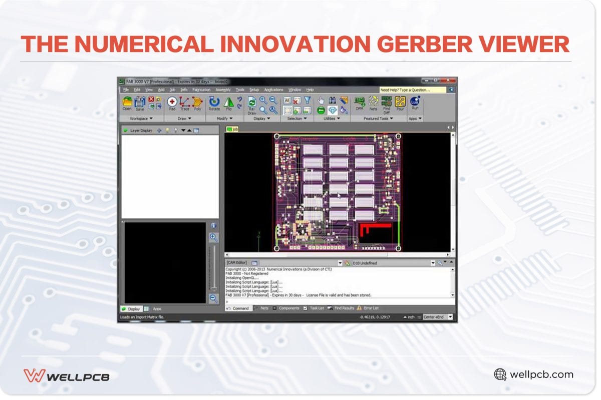
The Numerical Innovation Gerber Viewer
Numerical Innovation is simply awesome. This tool has checked all the highlighted features as important aspects of an ideal Gerber Viewer.
Are you looking for clarity? Check that. How about the ability to zoom images?
Please check that. Also, please check file compatibility. Honestly, an experience with Numerical is seamless.
The Eagle and the Altium-generated files from Seed Studio are very easy to use. For beginners, this could be an indispensable tool.
2.3 Common Issues and Solutions
The most common issues with Gerber files include:
- PCB design does not match the manufacturer’s capabilities
- Design file mismatch
- Insufficient clearances between pads and traces
- Incorrect, misaligned, misplaced, or missing layers
- Obsolete file formats
- Incorrect drill file format
- Inconsistent unit measurements
- Not providing fabrication drawings
- Duplicate or overlapping objects
- Missing board outlines
- Unintended copper pours
- Empty or corrupted/incomplete Gerber files
- Incorrect file naming conventions
- Unorganized file names/labels
- The composite layer does not map to a single layer
- Wrong CAD setting in the Gerber viewer
- Vectorized pads
- Multiple aperture lists
Some of the best practices to follow to avoid these Gerber file mistakes include:
- Do Thorough Design Reviews: Always do this before generating Gerber files to eliminate issues like misaligned/missing layers, overlapping objects, and incorrect aperture definitions.
- Use Dedicated Gerber File Viewers: This helps to check and validate each of the generated files (should inspect for things like missing layers, incorrect alignment, etc.)
- Use The Design Rule Checks in the PCB Design Software: Helps to identify any potential problems before generating the Gerber files.
- Follow the Naming Conventions: Stick to the established naming conventions for Gerber files and PCB layers to eliminate confusion and uphold organization.
- Use Consistent Measurement Units: Check and ensure all design and Gerber files have consistent measurement units in the entire design project.
- Check the Drill Files: Double-check these files to ensure they accurately outline the required holes and their sizes.
- Version Control: This helps to keep track of changes, revert to older versions in case of mistakes, and maintain a clear audit trail
- Collaborate with your Manufacturer: Lastly, always communicate with your contract manufacturer to clarify any required information, provide instructions/additional requirements, give design specifications, etc.
Chapter 3: PCB Fabrication Process
The PCB manufacturing process requires these 6 steps.
3.1 Pre-Production Engineering
The customer sends the design document, which is then submitted to the engineer for review and to produce an accurate quotation. We help confirm whether the production documents are missing or wrong and determine the process steps and associated checks.
3.2 Lamination and Imaging
The lamination process requires these steps.
- Cut Lamination: Cutting and laminating according to the size of the finished board or the size of the panel
- Drying: The primary purpose of drying is to remove the moisture in the board and prevent it from warping during processing. Generally, it is dried at 150℃ for 3-4 hours.
- Inner Layer Imaging: Inner dry film application, exposure, then development (exposed core plate is developed, the unexposed dry film is set to reveal the original copper skin, and the exposed dry film is retained)
This is followed by chemical etching, which corrodes the exposed copper to leave the copper trace patterns.
3.3 Drilling and Plating
Drilling can either be done using lasers or mechanical tools to create through-holes that will be plated to form vias or plated through holes. Lasers give better control over the drilling process, making it possible to form tiny microvias, blind, and buried vias.
The next step is to plate these holes, which is done using Electroless Copper Deposition (ECP) and Horizontal Electrolytic Plating (HEP). HCP coats a skinny layer of copper through the chemical reaction, about 2-3 um, while HEP can be used to thicken the copper in the gap and base plate to 5-8um using an electron transfer reaction.
3.4 Outer Layer Imaging and Etching
A dry film is applied to the bare copper core board, and all photo image reactions are performed on the dry film. The hole is drilled into the plate; the dry film is attached to protect the spot.
Next is outer layer development, which differs from the development of the inner layer because the copper under the dry film is the last to be retained after the inner layer is developed.
After the outer layer is formed, the copper of the dry film is the previous copper to be etched, and the copper that needs to be preserved is exposed at this time. But Tin is used to protect the desired copper during this stage.
3.5 Solder Mask and Silkscreen
We coat the entire panel with a liquid solder mask. The board is then exposed to high-intensity UV light. The solder mask protects copper circuitry from oxidation, damage, and corrosion. WellPCB prints the solder mask under customers’ requirements and does not have an extra charge.
Silkscreening is the next vital step since this process prints essential information onto the board, then the PCB finally passes through the coating and surface finishing process.
3.6 Surface Finish and Profiling
Surface finishes provide protection and good solderability. Joint surface finishes include Electroless Nickel Immersion Gold (ENIG), Hot Air Solder Leveling (HASL), Lead-Free HASL, Immersion Silver, OSP, etc.
Following the implementation of the Rohs directive in the EU, all products containing lead and bromine will not be allowed to enter the EU market; therefore, the traditional pewter process will be gradually replaced.
WellPCB defaults to the lead-free HASL for our customers. If you need to deal with it in a different way, please check the box when you place the order.
For profiling, our engineering department then creates a shape program based on the border provided by the customer. The shaping process is based on the engineering department providing milling.
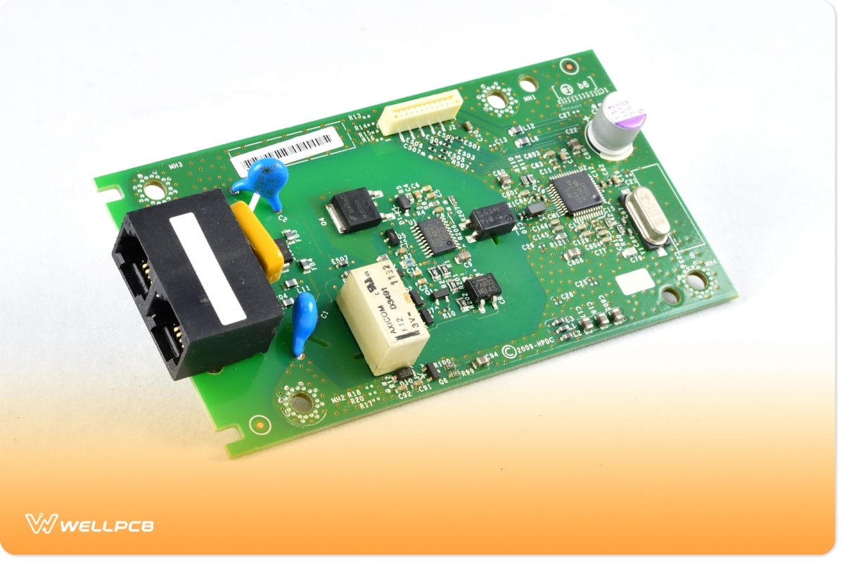
Chapter 4: Final Testing and Quality Control
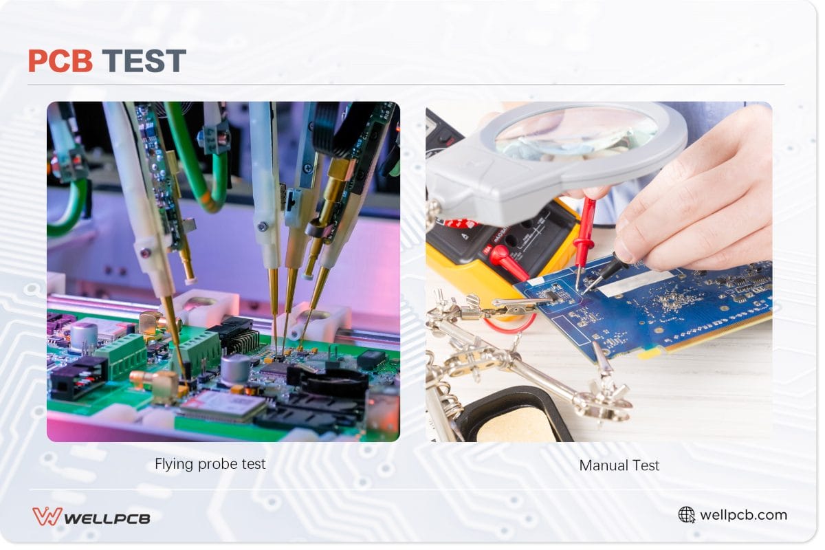
Image: PCB Test
4.1 Electrical Testing
So far, the board production has been completed, but another important thing is to conduct electrical testing to ensure functionality. The main tests that are performed are the circuit continuity and isolation tests.
Basic electrical reliability testing is used for checking the integrity of the tracks and the through-hole interconnections-checking to ensure there are no open circuits or short circuits on the finished board.
WellPCB uses Flying Probe Testing to test the electrical performance of each net on a bare circuit board. To ensure optimum performance and quality, we check each net to ensure it is complete (no open circuits) and does not fall into any other trap.
4.2 Visual Inspection and Packaging
Visual inspection is the final step in the PCB fabrication process. The professional quality control team will perform the final inspection of each PCB, including visual inspection, finished product size inspection, aperture hole number measurement, warpage measurement, etc. We will print a test report for customer reference if the review is qualified.
After inspection, the PCBs are vacuum-sealed to keep out dirt and moisture. They are then securely boxed, sealed, and shipped by courier to customers all over the world.
WellPCB suggests DHL and FEDEX, which are more convenient and fast – generally 1-4 Days so you can receive the board as soon as possible and start your project soon.
Conclusion
To wrap it up, PCB design and manufacturing are two of the three critical processes required to make these electronic circuits function as required and run reliably for years to come. The third is PCB assembly.
But these processes are advancing to make the manufactured boards have a higher quality, and one of the steps that is being looked at is etching.
The current standard is to use chemicals (acids) to corrode the unwanted copper, which is a toxic process and challenging.
As techniques like dry/laser etching and additive manufacturing advance, this process should become less toxic and more precise.
In the meantime, you should apply the insights we’ve shared above, especially during PCB design (layout and stackup), because these form the foundation of the board.
We can help you design your circuits or check them once you send your files.
And you can be sure of constant communication from us to fine-tune your designs before we commence the manufacturing process.
So, if you’re ready to get started, contact us and we’ll be in touch ASAP.