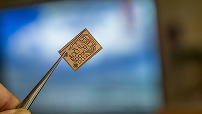
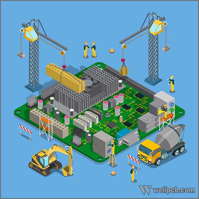
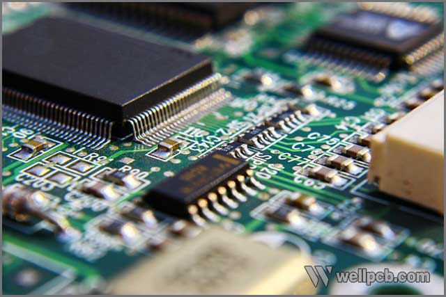
It is essential to be careful when designing your PCB for any purpose. Many designers have specific methods when designing circuit board components. But it may not be comprehensive. Some complex problems can be solved. This article will talk about printed circuit board assembly in detail and help you get your desired results. Now without much ado, let us get started:
Contents
- 1 Printed Circuit Board Assembly–Use the Right Design Tool
- 2 Printed Circuit Board Assembly–PCB Component Placement
- 3 Printed Circuit Board Assembly–Eliminate or Minimize the Use of Vias
- 4 Printed Circuit Board Assembly–Ensure Components and Packages are Consistent With BOM
- 5 Printed Circuit Board Assembly–Mark the Orientation of Components and Connectors
- 6 Printed Circuit Board Assembly–Use a Heat Sink in a Flat Surface
- 7 Printed Circuit Board Assembly–Be Careful About the Size
- 8 Printed Circuit Board Assembly–Go For Small Loops
- 9 Printed Circuit Board Assembly–Consider Noise Sources
- 10 Printed Circuit Board Assembly–Select Correct Materials
- 11 Printed Circuit Board Assembly–Pay Attention to Grounding
- 12 Printed Circuit Board Assembly– Always Go For a Prototype
- 13 Conclusion
Printed Circuit Board Assembly–Use the Right Design Tool
Before you sit down to design or assemble your printed circuit board, you will have to think about how you want it to turn out.
Most designed using a variety of tools for this purpose, including some exclusively designed for PCB such as Framer X. It creates interactive prototypes in large numbers, but this is not your only option, as there are other popular tools such as TinyCAD, Eagle PCB, and CircuitMaker.
If your prototype design does not highlight what you expect from the end product, then the company you have hired to do the job will never provide you the results you expect. Hence, expect a reasonable amount of time here.
If you are a novice with no understanding of design tools, you can choose to work with a company willing to provide you options. Most professional prototype PCB assembly providers have experienced designers who can get the job done for you.
Printed Circuit Board Assembly–PCB Component Placement
The PCB design is 90% layout and 10% wiring,this is entirely accurate. Taking the time to place your components accurately will make your life easier, which involves time to route everything.
• waste time
When you find that some parts do not even have enough space to route, You might make a mistake because they are too tightly together. Worst assembly placement may result in the need to restart the entire circuit board from the beginning.
• Broken
Suppose you did drop some components and traces and then send the file to the manufacturer. Next, you know you might get a circuit board back because your parts are not soldered properly (this will be covered in detail later), so this will not work.
• Ugly aesthetics
Let us face it because we like symmetry and precision; there is nothing more disturbing than the circuit boards an engineer sees without proper care and attention during component placement. Just lazy.
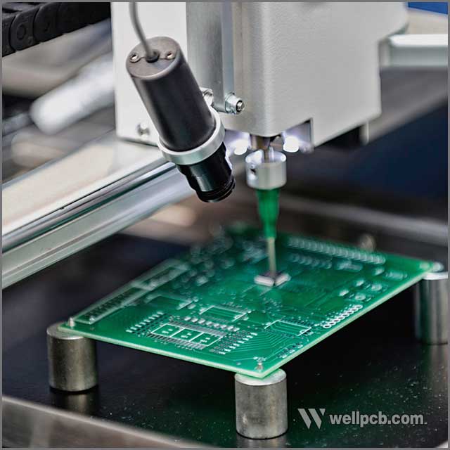
Printed Circuit Board Assembly–Eliminate or Minimize the Use of Vias
When it comes to printed circuit board assembly, you can choose from three vias, including through-hole vias, blind vias, and micro vias. They differ in functionality and price, but they all do the same thing.
We suggest opting for through-hole vias instead of buried vias or laser vias if you want to keep costs under control. Vias are essential because poor selection will impact the end product is interconnectivity. Plus, it also largely influences the overall cost.
Through-hole vias penetrate from the top to the bottom layer to establish a complete connection. This option can be either NPTH or PTH.
The rest of them use more vials, hence ending up costing more and can also be a little complicated to handle.
Printed Circuit Board Assembly–Ensure Components and Packages are Consistent With BOM
In the world of printed circuit board assembly, a BOM, short for a bill of materials, is an ingredients list you will need to build your product, the board in this case. BOM is used to buy products because you will need it throughout the process to ensure you get the right end product. You may have to send one to the company you hire to get the job done.
It will help you determine the number of factors, including:
- Lead-time to procure the materials
- Manufacturing processes
- Cost of Goods Sold (COGS)
- Quality of the Design for Assembly
- Cash flow requirements
- Supply chain robustness
Hence, it is essential to ensure components and packages are exactly how explained in the BOM.
Printed Circuit Board Assembly–Mark the Orientation of Components and Connectors
Connectors, especially through-hole connections – present significant opportunities for errors in both assembly and layout.
The layout specialist may not always know which site to place the connector. Moreover, it would help if you also were clear about where to put the hole. It is not as evident as it appears; hence marking orientations and location is critical.
Clear marking reduces the risk of errors and ensures that you get the results you expect when the final product arrives.
Printed Circuit Board Assembly–Use a Heat Sink in a Flat Surface
In printed circuit board assembly, heat sinks are essential because the regular flow of current can cause the board to heat up, affecting performance and even leading to damage to one or more electrical components.
The purpose of a heat sink is to control heat and minimize internal temperature so that the unit can continue to run for longer.
Altering exchange surfaces or using fans are the two best ways to control heat. It turns out that the radiator can effectively control the temperature, but must carefully choose. Here are a few things to keep in mind:
- The material should be selected with care. Aluminum and copper are the top two choices, but the right one depends on choosing the board.
- Fin configuration needs special attention as the layout and geometry of fins to play an essential role in how heat dissipates.
- The footprint must be kept under control since a considerable heat sink can put stress on the board and even cause further damage.
- Fin height needs to be paid attention to as well. However, Since in some cases, it may require shorter fins, and therefore a tradeoff.
l How you attach the sink also plays a vital role in the overall performance. Choose a suitable method if you want good results.

Printed Circuit Board Assembly–Be Careful About the Size
Before you get down to building PCB boards and completing other printed circuit board assembly tasks, it is essential to know exactly where you intend to use these and how.
These tablets are used for everything, from televisions to laptops. However, since the electronics’ size and design mainly differ, one PCB board may not always fit others.
Special tools for the size of the tracking device. Also, this should be done before you design, Because you need to design according to size. The finished product must fit your essential space. Otherwise, it may not be of use.
Printed Circuit Board Assembly–Go For Small Loops
The traces that you point are called loops, and they need to be small; otherwise, they will create noise, resulting in disruption.
You should remember this point during the design stage and must pay special attention to it whenever you stack a new layer or consider grounding as every addition may affect loops.
Printed Circuit Board Assembly–Consider Noise Sources
Electronic noise in PCBs can negatively affect the operation of the board. Hence it needs special attention, mainly if our circuit operates at frequencies in MHz or higher.
Higher frequencies increase the risk of noise that can cause the performance to degrade. The best way to reduce noise is to pay attention to potential sources and nip the bud’s evil during the designing phase.
Nonetheless, here are some tips to control the noise:
- Cover as much area of the board as possible with power planes and ground.
- Keep original single traces as small and thin as you possibly can.
- Make sure to place the digital and analog circuitry separately on the board.
- Avoid going for 90-degree turns; instead, choose two 45-degree turns if required to have a 90-degree twist.
- Make sure to place traces away from oscillators.
Printed Circuit Board Assembly–Select Correct Materials
You will need several materials to complete aboard. These include FR-2 (phenolic cotton paper), FR-3 (cotton paper and epoxy), FR-5 (woven glass and epoxy), FR-4 (spun glass and epoxy), FR-6 (matte glass and polyester), CEM-1 (cotton paper and epoxy), G-10 (woven glass and epoxy), CEM-2 (cotton paper and epoxy), etc.
There are several varieties of all these options. Since you will probably hire someone else to manufacture the board on your behalf, you may not have full control over the materials used. Still, it is essential to discuss this factor with the provider and be on the same page regarding expectations and delivery to know what to expect in the end.
Printed Circuit Board Assembly–Pay Attention to Grounding
Grounding is a concept that gets involved whenever we talk about items that deal with an electric current. Each PCB requires proper grounding to function correctly.
It can be defined as a grounding conductor, either as an arbitrary node voltage potential, And can combine the loop current.
What gets called a ground depends on the design of the board. Poor grounding can reduce performance. Hence it is essential to control the flow of current.
You can choose from multiple choices, including:
- Floating Grounds
- AC Grounds
- Virtual Grounds
- Earth Grounds
- Chassis Grounds
However, when it comes to PCBs, the choices end up being a ground plane, ground plane vias, connector grounds, and decoupling.
You can choose one of these options based on your requirements but make sure to remember the following tips:
- Ensure you attach everything
- Remember to keep the ground layer whole.
- Always have a common ground point.
- Use as little series vias as possible.
- It is better to design grounding before you move to the route.
- Sit down and carefully understand all about how your currents flow.
- Plan how you wish to handle dynamic variance between multiple grounds
- Design keeping in mind mixed-signal considerations
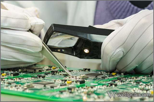
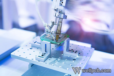
Printed Circuit Board Assembly– Always Go For a Prototype
Once you have selected a company, it is best to first request a prototype to handle printed circuit assembly. I will ensure you are well aware of what you are opting for because not all companies deliver what they promise.
Most printed circuit board assembly companies are willing to provide PCB prototype assembly if you promise to give a large order in return.
Conclusion
Now that you know how to design for optimal circuit board assembly, we’re sure you will have no problems getting what you want. Get in touch with us today if you’re ready to get high-quality boards manufactured.