
Contents
- 1 What is the Rigid-flex PCB?
- 2 Rigid-Flex Layer Stack Type Design
- 3 Application Range of Rigid-flex PCB
- 4 Guidelines for Rigid-flex Design.
- 5 What Material Should You Choose for Rigid-Flex PCB Design?
- 6 Software for rigid-flex PCB Design
- 7 Precautions for rigid-flex PCB Design
- 8 Rigid-flex PCB Design Frequently Encountered Problems.
- 9 Summary:
What is the Rigid-flex PCB?
As the name suggests, a rigid-flex printed circuit board (RFP) is a hybrid board that uses an integration of flexible and rigid board technologies in an electronic application. Almost all rigid-flex PCBs design a flexible polyimide component on a fixed Flame Retardant type 4 (FR4) stiffener.
You will discover that some parts of the board are flexible while others are rigid upon examination. What’s more, you can easily bend or fold the circuits and still maintain the shapes of areas that require more support.

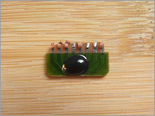
(The high-tech background of rigid-flex PCB)
Rigid-Flex Layer Stack Type Design
The manufacturer designs the PCB as a multilayer stack to define each layer’s layout vertically, also known as the Z plane. The layer stack has a fabrication of a single unit on any board.
The best layer-stacking strategy
A perfect layer stack-up strategy should enable you to arrange traces and ground planes to block EMI. Furthermore, it should adapt to the rigid-flex design and the design’s temperatures.
A multilayer stack is desirable. It is because of the following reasons;
- It can alternate between signal and ground planes.
- Each of its layers has a dielectric or a prepreg in between them.
- It considers thermal problems.
- It accommodates devices with analog and digital elements. However, the devices are to use separate ground layers in the stack-up. The essence of separation is to avoid noise coupling and prevent EMI.
Single-layer features
- Has one or two polyimide outer cover layers.
- It has holes that are accessible on one or both sides.
- Component holes lack plates.
- You can use components, stiffeners, pins, and connectors on a single-layer type.
- Highly recommendable in applications dealing with static and dynamic flex.
Double-layer features
- Designers plate through the holes hence allowing connection to take place between the two layers.
- You can use components, stiffeners, pins, and connectors even though there may be an absence of stiffeners.
- There’s the presence of two conducting layers with an insulator sandwiched between the layers. Designers may cover the outer layer or leave the pads open.
- The uncovered pads or access holes are on both sides- vias can have covers on both sides.
- Applicable for stationary and active flex applications.
Multilayer features
- First, multilayer PCBs have three or more flexible conductive layers. Designers then place a flexible insulating component between each layer. Lastly, they may choose to cover the outer layer or expose the pads.
- The via can be covered or exposed as well.
- Contact holes or the free pads are on either or both sides of the PCB.
- Various materials are utilizable, for instance, components, stiffeners, pins, and connectors.
- Often found in static flex applications.
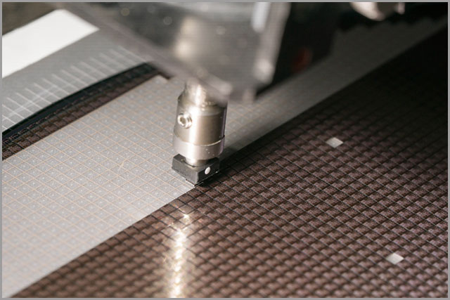
(close up on a multilayered PCB)
Application Range of Rigid-flex PCB
RFP has a wide range of applications in electronics and sometimes in control systems. Depending on the product it is used on, you will find its application in;
- consumer appliances
- automotive industry
- aerospace industry
- Control tower systems
- CCTV surveillance systems
- industrial automation systems
- control panels

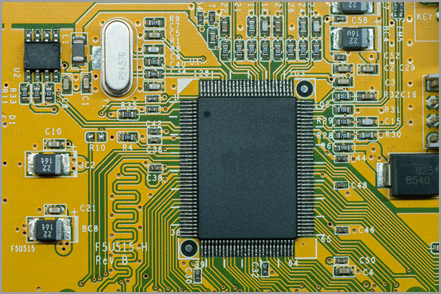
(an example of rigid-flex PCB application on a motherboard)
Guidelines for Rigid-flex Design.
Without the proper guidelines in assembling/ designing your RFP, the final product can be prone to challenges. Therefore, following the stipulated instructions in the letter can save you a huge deal.
The following are some standard guidelines that you can follow when designing your PCB.
- First, prepare the material type (adhesive, conductor, etc.), manufacturing method (whether pressure and heat are required), and the number of layers.
- Second, make sure to place the copper traces at a 90° angle of rigid and flexible bends.
- Then, consider the electrochemical factors affecting both the flex circuit and rigid board. Regarding that, you will need to focus on the ratio of bend radius to thickness. As a rule, the bend radius should be a minimum of ten times the flex material’s thickness.
- Moreover, you ought to leave a distance of 0.5 mm between the copper annulus and adjacent vias. A close connection can cause fatigue that often occurs after frequent bending. Again, the vias should be in motionless areas on the board, i.e., where they rarely move.
- Lastly, check the product operating conditions. To put it another way, check for ambient conditions, for example, temperature change, cooling, humidity, shock, non-flammability, and vibrations.
(colorful illustration of a rigid-flex PCB)

What Material Should You Choose for Rigid-Flex PCB Design?
Substrate and Cover films
The preferable type is woven fiberglass sandwiched in epoxy resin. The fiberglass has a certain degree of elasticity. On the other hand, cured epoxy makes the board appear rigid. Using epoxy requires a state where there’s less movement.
Polyimide is a substitute for epoxy because of its improved flexibility. Furthermore, you can’t easily tear this material or stretch it by hand. Finally, it is highly resistant to heat, thereby maintaining stability during fluctuations in temperature.
Polyester (PET) is often commonly applicable during the design. A downside with this material is the fact that it can’t survive for long in extreme temperatures. Thus, you’ll find its application in low-cost electronic products.
Polytetrafluoroethylene (PTFE) may act in the place of a PET. You will mostly use it in high-frequency products with low dielectric constant.
Coverlay acts as an insulator and protects the outer surface from harm and unwanted deterioration.
(close up on an epoxy resin)
Conductors
Choices vary from carbon film and silver-based ink, but the most preferable is copper. The copper choice will most definitely go with its application. For instance, a laminated copper foil (Electro-Deposited) is appropriate in simple, flexible circuit parts or heavyweight coppers fit in to keep high-current carrying conductors.
Another conductor in the market is the Rolled Annealed (RA) foils. It has a higher cost than the standard copper, but the quality of stretching and springing is superb.
Adhesives
Adhesives are for flexibility. Its function is to bond the copper foil to polyimide or other films since heat and pressure alone can’t form a dependable connection. Materials used include acrylic or epoxy-based adhesives with thicknesses of about 0.5-1 mil.
You can also use silicones and hot-melt glues in flex and rigid interfaces.
(use of silicone)
Software for rigid-flex PCB Design
You can use the software in PCB designs to animate and distinctively define your PCBs. Here are two known ways in which you may jumpstart the process:
Integrated ECAD/MCAD tools
ECAD/MCAD enables bi-directional collaboration between electrical and mechanical domains. The tools visually validate designs with photorealistic 3D to reduce iterations. They simplify the designing process by checking for the following.
Altium Designer
Altium Designer’s PCB is a layered design setting that supports about 32 signal layers and 16 plane layers. Inarguably, the advanced Altium Designer is the only PCB design software with the ability to give you the necessary tools for rigid-flex PCB assembly in a single platform.
Alternatively, Altium Designer comprises a powerful 3D rendering engine that presents a realistic 3-dimensional representation of the circuit board. The engine supports rigid-flex circuit boards, and it can examine the board in a flat state.
Precautions for rigid-flex PCB Design
Failure to follow guidelines can result in disastrous aftermath. What’s more, it can lead to a wastage of materials, time, and money should you miss a step in the procedure.
There are a few general precautions that you’ll need to keep in mind before the designing process, and they include;
- Avoid bending at the corners. Should you do so, ensure the corners are curved, not sharp.
- You should not place components or vias close to the bend line. The bend lines affect routing by causing material stress.
- Use hatched polygons to maintain flexibility when carrying a power or ground plane on the flex circuit.
- Progressively change the width of the traces. Sudden changes in trace widths can lead to a weak spot.
- Keep the flex layers to a minimum of two for maximum flexibility and low cost.
- Use a printed circuit board with the lowest thickness and reduced material types. A thick RFP affects the miniaturization of assembly products and consequently inconveniences the manufacturing process.
- The arrangement of the wires shows the folding resistance requirements to enhance the shock resistance.
Rigid-flex PCB Design Frequently Encountered Problems.
- Flexible PCB bending radius and position
When the board bends over a long period, some flex circuitry parts will have extra stress more than their counterparts. A less-rounded radius also contributes to physical stress.
- There can be problems involving the mechanical requirements for rigid-flexible PCBs. It is concerned with the circuit board thickness (thick boards are inefficient), bending form, bending frequency, and drill hole diameter ratio to board thickness.
- If you don’t correctly place the space between a pad and copper trace, there can be shorts. Hence, the distance should be able to house the mask.
- Stacked traces found on a similar spot on the opposite side of dielectrics experience stress due to their position, which tragically causes them to fracture. It appears to be a sentence fragment. Consider rewriting it as a complete sentence.
- Designers can cause underlying damage traces in cases where they apply an excessive amount of cover film on the PCB.
Summary:
All in all, taking precautionary measures presents a higher percentage of effectiveness in the PCB design. Such action is commendable since it saves on cost, lengthens the board’s lifespan, and in an overall aspect, maintains the quality of the plan.
We do hope you’ve gained some basic rigid-flex knowledge from this article. In case of inquiries, concerns, or comments, kindly get in touch with us. Indeed, we will be more than glad to have you on board in our gradual learning session.


