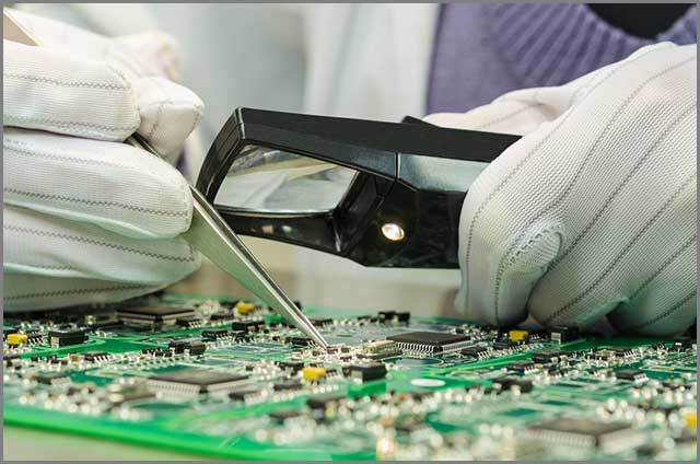
PCB failures can happen in an electrical connection between elements due to many reasons. For instance, PCBs’ speed of operation has increased dramatically, leading to a more complex PCB layout and more dense circuits. As a result, many manufacturing issues have arisen, considered a big problem for PCB manufacturers.
This article will discuss the common reasons for PCB failures, short circuit Protection in PCB circuit design, and avoid both. Additionally, we present a brief guide on preventing short circuits in PCB circuit design and how designers can reduce the possibility of PCB short circuit protection.
Contents
- 1 1. The common reasons for Printed Circuit Boards Failures
- 2 2. Short Circuit Protection– How to avoid Printed Circuit Boards Failures
- 3 3. Short Circuit Protection in PCB Circuit Design
- 4 4. How to Prevent in PCB Circuit Design
- 5 5. How Can Designers Reduce the Possibility of PCB Short Circuit Protection?
- 6 Conclusion
1. The common reasons for Printed Circuit Boards Failures
1.1 Short Circuit Protection–Burnt Circuit Board
In the production phase, PCBs typically go through various manufacturing steps that involve applying high temperatures. It is crucial not to expose the PCBs to extreme temperatures, as it may cause severe damage to the circuits’ electronic components severely. Each of the electronic components integrated into the PCB has a specific temperature to withstand without being burnt. These components are very prone to be damaged through unregulated temperatures. Another thing to keep in mind is that each component should have enough space around it to avoid burning caused by overheating.
1.2 Short Circuit Protection–Poorly Manufactured Components
The need to produce an overwhelming amount of microelectronic parts in a limited time has made it challenging to ensure the high reliability of the PCB components. Obvious manufacturing flaws in PCBs are connection failures, residual flux, and bad soldering, which can be an annoying source of trouble later on. That often leaves the PCB manufacturers with no choices except to increase their validation techniques to guarantee high-quality final products.
1.3 Short Circuit Protection–Environmental Factors
As previously mentioned, PCBs contain electronic components that are typically small in size. Additionally, these electronic components (e.g., ICs) are sensitive to the surrounding environment, and they are vulnerable to unforeseen changes in temperature, humidity, and dust levels. For instance, unexpected temperature changes may lead to wrapping the PCB board and the soldered joints. An excessive amount of dust will not allow the PCB to cool appropriately, resulting in overheating issues.
1.4 Short Circuit Protection—Plating Voids
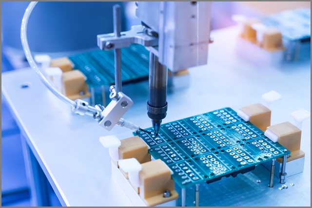
To enable powerful and high-speed products, PCB manufacturers prefer to use multilayer PCBs with many components. Multilayer PCBs play critical roles in electronic systems; we can think of it as multiple PCBs joined together. Generally, we interconnect the multi-layers of PCB by the plated-through holes (PTH) and buried/blind vias. Unfortunately, this can quickly fail because PTH’s penetration is usually higher than that of the blind via and buried. PTH’s condition and accuracy undoubtedly affect the reliability of PCBs, even the performance of the whole final product.
1.5 Short Circuit Protection—Missing Solder Mask Between Pads
It is crucial to insulate copper traces in PCBs to avoid accidental contact with other conductive materials. Therefore, we typically form a soldering layer (mask) on top of the PCB’s copper layer to act as an insulation layer. This insulation layer is also useful in preventing corrosion and protecting the board from other environmental changes. By pads, we mean the metal space left uncovered by the soldering board, which the PCB components are attached to. The soldering insulating mask may be missing between the pads, resulting in solder bridges between pins. One of the common issues arising from this is the formation of short circuits and corrosion.
2. Short Circuit Protection– How to avoid Printed Circuit Boards Failures
We can sidestep PCB flaws resulting from contamination by cleaning the board appropriately after drilling. Moreover, we can avoid drilling failures by following the drilling regulations recommended by the manufacturer. Dealing with an experienced PCB company can prevent us from both of these problems. In the process of forming the solder mask, thin copper wedges may appear. That is usually spotted by a DFM test and can be prevented by ensuring that each section has a minimum width.
In complex PCB products with multiple layers, we must verify that the layers are correctly aligned by following the acceptable standards for the type of board being used, as failing to do so results in open and short circuits affecting the functionality of the product.
3. Short Circuit Protection in PCB Circuit Design
The term short circuit refers to an event in which the electrical current passes through an unintended path with almost zero resistance, resulting in excessive electrical current flow in the circuit. In PCBs, short circuits happen when two conductors are connected unintentionally, causing unrelated signals to be mixed, or even worse, causing the connection to be damaged.
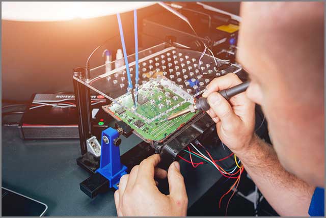
We can identify short circuits with our naked eyes if the short circuit is between two thick wires; however, in many cases, it is hard to identify short circuits, especially if the wires are so small. In machine-produced PCBs, the wires are tiny, and we need to use more advanced techniques to detect short circuit failures.

4. How to Prevent in PCB Circuit Design
Unfortunately, detecting short circuits in machine-produced PCBs can be a real headache for manufacturers. It is very time-consuming, and it can cost more than the whole assembled PCB board! Short circuits are a kind of problem that cannot have zero occurrence probability.
In other words, we cannot avoid it, but we can use preventive practices to reduce its probability of occurrence. To detect the short circuit defects, we can use X-ray inspection methods. However, these test methods may not be used in production tests since they take a long time. Also, even if a change in the shape of a solder ball occurs, logic signals may be propagated as expected.
Thus, some overkill may occur in the tests. We can also utilize a boundary scan examination method since short circuits can generate faulty logic signals. However, it is difficult to estimate the faulty effects. Thus, even if the test method is used for detecting these flaws, they may not be detected. Also, it may be difficult to locate the connected leads.
On the other hand, post-production electrical testing is one of the best checking methods to detect short circuits. It does identify not only short circuits but also reveals errors that originated from the design. This kind of testing is typically done using flying probes.
We should always keep in mind that the PCB testing methods do not have 100% accuracy, and the short circuits can escape the testing procedures. However, testing PCB is always beneficial, and it prevents damaged PCBs from being assembled and sent to advanced steps.
A normal procedure ensures that you have a reimbursement policy with your manufacturer that guarantees you are reimbursed for when the PCB fails the electrical testing.
5. How Can Designers Reduce the Possibility of PCB Short Circuit Protection?
In general, we can assume that the PCB failures caused by short circuit defects are a fault of the PCB production process. However, designers can follow preventive design procedures to reduce the likelihood of these faults.
We most probably encounter short circuits in sophisticated PCB designs, including numerous components. As a result, allowing a larger space between copper connections and pads is one of these preventive actions, but sometimes this is not possible because of the design constraints.
Designers can use advanced design software to set clearance rules and modify the minimum allowed spaces before deciding to complete the design process and send it for manufacturing.
Conclusion
The density of the PCB designing and production procedures means there are plentiful chances for PCB defects to arise. Some of these issues are because of the design mistakes, such as inadequate clearances or spacing between components, which can harmfully affect the final PCBs’ functions. Others may come from mistakes in the production process, such as drilling faults or over-etching, which can be very costly and time-consuming catastrophic.
In WellPCB, our engineering team is committed to delivering outstanding final products with high-quality PCBs having minimal defects. We will provide you with a one-stop service and high-quality products. You can send us the documents you need to make and get a quote immediately! What are we waiting for? We have ten years of PCB manufacturing services. Please find out more about our WellPCB.
Reference:
Videos